· Priya Nair · Engineering · 6 min read
DFM for Fine-Pitch BGA
Master DFM rules for fine-pitch BGA packages (≤0.5mm pitch). Covers pad design, solder mask opening, via-in-pad requirements, and common assembly defects with prevention strategies.
Quick Answer
Fine-pitch BGA DFM requires three non-negotiable rules: (1) copper-filled and planarized via-in-pad for all BGA pads that cannot escape-route between pins, (2) LDI solder mask registration for ≤0.5mm pitch to maintain minimum 50µm mask dams between NSMD pad openings, and (3) proper stencil aperture reduction (80-90% of pad area) to prevent solder bridging. NSMD pads are preferred over SMD for better solder joint strength and consistency.
The DFM Challenge of Fine-Pitch BGAs
Ball Grid Array (BGA) packages below 0.5 mm pitch represent one of the most demanding challenges in PCB design for manufacturability (DFM). At 0.4 mm pitch, the pad diameter shrinks to approximately 200–250 µm with only 150–200 µm spacing between pads — leaving no margin for design errors.
Assembly defects on fine-pitch BGAs are expensive. A single bridged joint can require $50–200 in rework for consumer products, or outright board scrapping for Class 3 aerospace/medical applications. The good news: most BGA assembly defects are preventable through proper DFM at the PCB design stage.
This guide covers the critical design rules that separate reliable fine-pitch BGA assemblies from costly yield problems, building on our general [SMT pad design]/blog/pcb-smt-pad-design-fine-pitch-en/) guidelines.
Pad Design: NSMD vs SMD
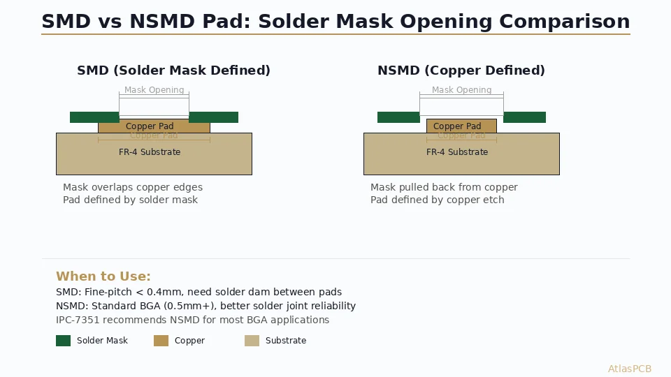
The first fundamental choice is between Non-Solder-Mask-Defined (NSMD) and Solder-Mask-Defined (SMD) pads.
NSMD Pads (Preferred for ≤0.5mm pitch)
The copper pad is smaller than the solder mask opening. The solder mask opening is larger than the pad by a defined clearance.
Advantages:
- Copper etching determines pad size (±12.5 µm typical)
- Better solder joint profile (solder wraps around pad edges)
- Higher shear strength (30-50% improvement vs SMD)
- More consistent pad size across the array
Design rules for 0.4mm pitch NSMD:
- Copper pad diameter: 200–220 µm
- Solder mask opening: 260–280 µm (40 µm clearance per side)
- Minimum solder mask web: 75 µm (between adjacent openings)
SMD Pads (Use when mask web is impossible)
At very fine pitches (<0.35mm), the solder mask web between NSMD openings may fall below the manufacturer’s minimum capability (typically 50–75 µm). In this case, SMD pads become necessary.
Design rules for SMD approach:
- Solder mask opening: 180–200 µm
- Copper pad: 250–280 µm (extends under mask)
- Registration tolerance becomes critical (mask-to-copper)
Via-in-Pad Requirements
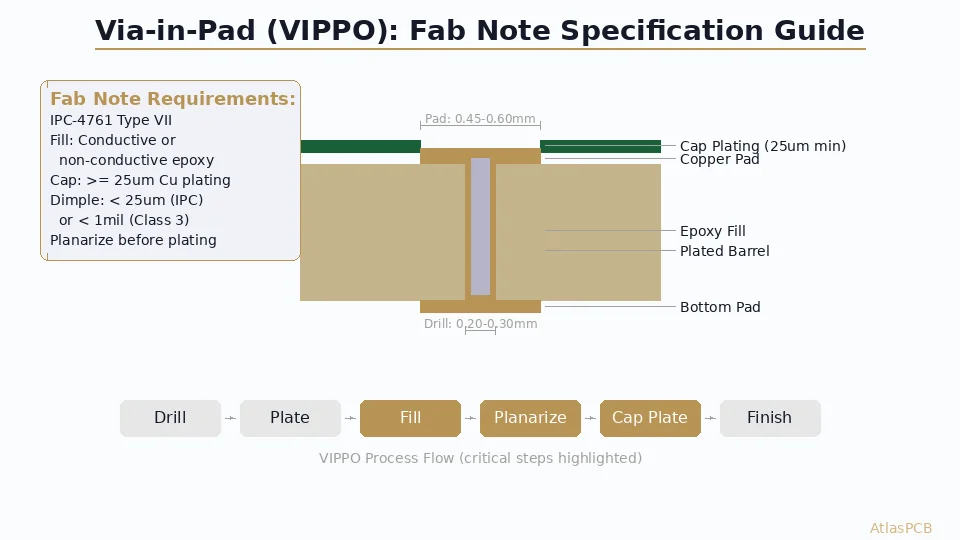
Fine-pitch BGAs typically require [via-in-pad design]/blog/pcb-via-in-pad-plated-over-design-en/) for signal escape routing, especially for interior rows that cannot route out between pads.
Why Via-in-Pad Is Necessary
At 0.4 mm pitch with 200 µm pads and 200 µm spacing, there is no room to place a via adjacent to the pad and route a trace between neighboring pads. Dog-bone fanout is only possible for the 2-3 outermost rows.
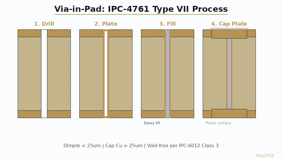
Copper-Fill Requirements
Vias in BGA pads must be:
- Filled with conductive material (copper or conductive epoxy)
- Planarized (cap-plated flush with pad surface)
- Void-free in the fill (voids cause solder wicking during reflow)
A via that isn’t properly filled will:
- Wick solder paste down into the via (insufficient solder on pad)
- Create voiding in the solder joint
- Cause opens or cold joints
This is why [resin plug via process]/blog/pcb-resin-plug-via-process-en/) quality is critical for BGA reliability.
Via Specifications
| BGA Pitch | Via Drill | Via Pad | Fill Method |
|---|---|---|---|
| 0.8 mm | 0.20 mm | 0.35 mm | Resin fill + cap plate |
| 0.5 mm | 0.15 mm | 0.28 mm | Copper fill preferred |
| 0.4 mm | 0.10 mm | 0.22 mm | Copper fill required |
| 0.3 mm | 0.075 mm (laser) | 0.18 mm | Microvia copper fill |
Solder Mask Design
Registration Tolerance
Solder mask registration is typically ±25–37.5 µm (1.0–1.5 mil) for standard processes, and ±12.5 µm for [LDI (Laser Direct Imaging)]/blog/pcb-laser-direct-imaging-ldi-en/) processes.
For 0.4mm pitch BGAs, LDI is strongly recommended to achieve the tight mask registration needed for consistent NSMD pad exposure.
Solder Mask Dam Between Pads
The minimum solder mask dam (web) between adjacent pad openings must meet fabrication capability:
- Standard lithography: ≥75 µm (3 mil)
- LDI process: ≥50 µm (2 mil)
- Advanced LDI: ≥37.5 µm (1.5 mil)
If your design cannot achieve minimum dam width, consider:
- Switching to SMD pad definition
- Removing solder mask between pads entirely (mask-less BGA area)
- Using larger NSMD openings with tighter mask registration (LDI fab)
For detailed mask dam calculations, refer to our [solder mask dam design rules]/blog/pcb-solder-mask-dam-design-rules-dfm-en/) guide.
Escape Routing Strategies
Layer Allocation
For a 0.4mm pitch BGA with 15×15 array (225 balls):
- L1: Outermost 2 rows escape (dogbone or direct)
- L2: Next 2-3 rows escape via microvias
- L3-L4: Interior rows escape via stacked/staggered microvias
This typically requires [HDI construction]/blog/hdi-pcb-stackup-design-advanced-en/) with at least 1+N+1 buildup.
Trace Width in BGA Field
At 0.4mm pitch with via-in-pad:
- Available routing channel: ~200 µm
- Trace width: 75–100 µm (3–4 mil)
- Space to adjacent pad: 50–75 µm (2–3 mil)
These are achievable with standard semi-additive processes but require manufacturing confirmation.
Common Assembly Defects and Prevention

1. Solder Bridging
Cause: Excess solder paste, pad-to-pad spacing too small, or solder mask misregistration.
Prevention:
- Use correct stencil aperture reduction (typically 80-90% of pad area for fine pitch)
- Maintain minimum mask dam or use well-registered LDI process
- Verify paste volume with SPI (Solder Paste Inspection)
2. Head-in-Pillow (HiP)
Cause: BGA ball partially oxidizes before full reflow coalescence, often due to warpage.
Prevention:
- Control reflow profile (minimize time above liquidus gradient across BGA)
- Specify low-warpage package orientation if possible
- Use nitrogen reflow atmosphere for fine-pitch BGAs
- Design thermal relief on thermal pads to reduce temperature gradients
3. Solder Voiding
Cause: Flux entrapment, via wicking, or outgassing from PCB/package moisture.
Prevention:
- Proper via fill (no unfilled vias in pad)
- [PCB baking]/blog/pcb-moisture-sensitivity-baking-en/) before assembly (especially for thick boards)
- Optimized stencil design with escape vents for large thermal pads
4. Opens (Insufficient Solder)
Cause: Solder wicking into unfilled vias, insufficient paste deposit, or pad co-planarity issues.
Prevention:
- Mandatory via fill + planarization for all BGA vias
- Verify stencil aperture size provides adequate paste volume
- Board flatness per [bow and twist specification]/blog/pcb-bow-and-twist-specification-en/) (IPC-TM-650: ≤0.75%)
DFM Checklist for Fine-Pitch BGA
Before releasing your design to fabrication, verify:
- Pad type documented (NSMD preferred, size specified)
- Solder mask opening ≥40 µm larger than copper pad (NSMD)
- Solder mask dam ≥50 µm (LDI) or ≥75 µm (standard)
- All BGA vias are filled and planarized
- Via fill method specified on fab drawing (copper fill for ≤0.4mm pitch)
- Escape routing verified with actual trace/space capabilities
- Stencil aperture recommendations documented for assembler
- Thermal pad design includes proper segmentation and venting
- Board thickness and layer count support required via structures
- [Impedance specifications]/blog/how-to-specify-impedance-pcb-en/) on BGA escape traces defined
Conclusion
Fine-pitch BGA DFM is fundamentally about respecting manufacturing tolerances while maximizing electrical performance. The three non-negotiable rules:
- Proper via-in-pad — copper-filled and planarized, no exceptions
- Solder mask control — LDI registration for ≤0.5mm pitch
- Validate with your fab — send your BGA area for DFM review before committing
At AtlasPCB, we provide free DFM review for complex BGA designs. Upload your files and our process engineers will identify any issues before they become production defects.
Further Reading
- [PCB Panelization and Array Design: V-Score vs Tab Routing, DFM Rules, and Cost Optimization]/blog/pcb-panelization-v-score-tab-routing-dfm-cost-optimization/)
- [PCB Manufacturer with Engineering Review: Why Human DFM Audit Matters]/blog/pcb-manufacturer-engineering-review/)
- [阻焊坝设计 — 规则、公差与DFM最佳实践]/blog/pcb-solder-mask-dam-design-rules-dfm/)
- [Aluminum PCB Thermal Design for High-Power LED and Motor Drivers: Material Selection, Stackup, and DFM Guide]/blog/aluminum-pcb-thermal-design-led-motor-driver/)
- [PCB Design for GaN and SiC Power Devices: Thermal Management, Layout Rules, and Material Selection]/blog/pcb-design-gan-sic-power-devices-thermal-layout/)
- Material Options & Capabilities
About AtlasPCB — We specialize in complex PCB manufacturing for HDI, RF, and high-reliability applications. Explore our HDI PCB manufacturing capabilities, free engineering DFM review, or get an full PCB manufacturing capabilities . Every order includes free engineering review. Get your quote.
Reviewed by AtlasPCB Engineering Team — IPC-certified manufacturing specialists with 15+ years of production experience in HDI, RF, and high-reliability PCB fabrication. Content based on factory floor data and real customer design reviews.
Frequently Asked Questions
What pad type should I use for fine-pitch BGA — NSMD or SMD?
Why do BGA vias need to be copper-filled?
What is the minimum trace width for BGA escape routing at 0.4mm pitch?
- DFM
- BGA design
- fine-pitch
- PCB design rules
- via-in-pad
- solder mask
- assembly defects