· Priya Nair · Engineering · 8 min read
Boundary Scan (JTAG) Testing for PCB Assembly
Learn how boundary scan (JTAG/IEEE 1149.1) testing verifies PCB assembly integrity, detects BGA opens and shorts without physical access, and integrates with flying probe and ICT for maximum fault coverage.
Quick Answer
Boundary scan (JTAG/IEEE 1149.1) testing uses dedicated test logic built into ICs to verify PCB interconnect integrity by shifting test patterns through serial scan chains, detecting opens, shorts, and stuck-at faults on BGA and fine-pitch connections that are physically inaccessible to bed-of-nails or flying probe testers — achieving 90%+ structural fault coverage when designed into the board from the schematic stage.
The Access Problem in Modern PCB Assembly Testing
As PCBs grow denser with BGA packages, 0201 passives, and fine-pitch QFN components, a fundamental testing challenge emerges: how do you verify that solder joints are good when you cannot physically touch the pins?
Traditional test methods — in-circuit test (ICT) with bed-of-nails fixtures and flying probe systems — require physical access to test points. But modern board designs have:
- BGA packages with hundreds of connections hidden under the package body
- Component-on-both-sides assemblies that limit bottom-side access
- 0.4 mm pitch QFP and CSP packages where probe tips cannot reach individual pins
- Dense routing that eliminates space for dedicated test pads
This is where boundary scan becomes essential. By leveraging test logic already built into digital ICs, boundary scan can verify every connection between JTAG-capable devices without any physical test probe access.
How Boundary Scan Works
The IEEE 1149.1 Standard
IEEE 1149.1 (commonly called JTAG, after the Joint Test Action Group that developed it) defines:
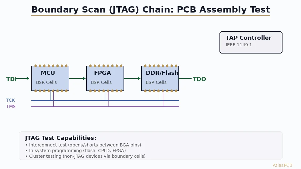
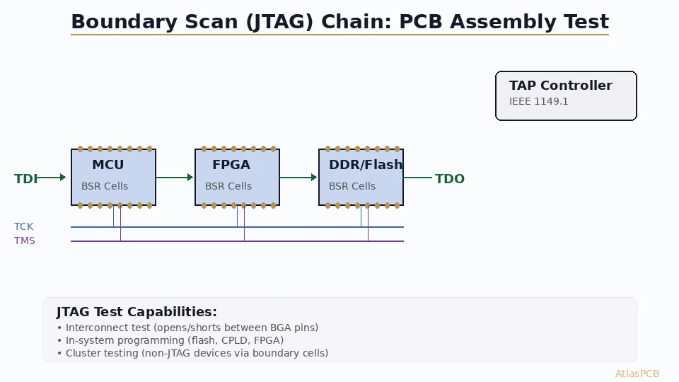
- Boundary Scan Register (BSR): A shift register cell at every I/O pin of a compliant device
- Test Access Port (TAP): A 4-wire (optionally 5-wire) serial interface for controlling the test logic
- TAP Controller: A state machine that sequences test operations
- Instruction Register: Selects what the BSR does (sample, drive, or bypass)
TAP Interface Signals
| Signal | Direction | Function |
|---|---|---|
| TCK | Input | Test clock — synchronizes all boundary scan operations |
| TMS | Input | Test mode select — navigates the TAP state machine |
| TDI | Input | Test data in — serial input to the scan chain |
| TDO | Output | Test data out — serial output from the scan chain |
| TRST | Input (optional) | Test reset — asynchronous reset of TAP controller |
The Scan Chain Concept
In a boundary scan implementation, multiple JTAG-capable devices are connected in a daisy chain:
TDI → [Device 1 BSR] → [Device 2 BSR] → [Device 3 BSR] → TDOTo test the interconnect between Device 1’s output pin and Device 2’s input pin:
- Load a known pattern into Device 1’s output boundary cell
- Drive that pattern onto the physical PCB trace
- Capture the value at Device 2’s input boundary cell
- Shift out and compare — if the captured value matches, the connection is good
This process happens simultaneously for all connections in the chain, testing thousands of nets in a single shift operation.
Types of Boundary Scan Tests
Infrastructure Test
The simplest test — verify the JTAG chain itself is intact:
- Shift a known pattern through all devices in the chain
- If TDO output matches expected pattern (delayed by total chain length), all devices are connected and functional
- Detects: broken TDI/TDO chain, dead devices, wrong device orientation
Interconnect Test (Most Valuable for Manufacturing)
Tests every connection between JTAG-capable devices:
- Opens detection: Drive a logic level on one device’s output, capture on the receiving device’s input. Mismatch = open joint
- Shorts detection: Drive opposite values on adjacent nets. If both read the same value, they are shorted together
- Stuck-at faults: Pins that always read high or low regardless of driven value
Cluster Testing (Testing Non-JTAG Components)
Boundary scan can test components that have no JTAG capability by using adjacent JTAG devices as drivers and sensors:
Example — Testing a pull-up resistor:
- Device A’s boundary cell drives the shared net LOW
- Read back through Device A’s cell: if the net reads HIGH, the pull-up resistor is connected and functioning
- If the net stays LOW: either the resistor is missing or the VCC connection is open
Testable non-JTAG components:
- Pull-up/pull-down resistors
- LEDs (drive and sense voltage drop)
- Bus transceivers and buffers
- Reset ICs and voltage supervisors
- Discrete transistor switching circuits
In-System Programming (ISP)
Beyond testing, the same JTAG interface enables:
- FPGA configuration (bitstream loading)
- CPLD programming
- Flash memory programming through JTAG-capable controllers
- Microcontroller firmware loading
This allows programming after assembly, supporting late-stage customization and field updates.
Design for Testability Review
AtlasPCB's DFT review ensures your JTAG chain routing, test point placement, and connector selection maximize boundary scan fault coverage before fabrication.
Request DFT Review →PCB Design Guidelines for Boundary Scan
Component Selection
When choosing components, prioritize IEEE 1149.1 compliance:
- Processors and MCUs: Nearly all ARM, x86, and RISC-V processors include JTAG
- FPGAs and CPLDs: All major vendors (Xilinx/AMD, Intel/Altera, Lattice, Microchip) support 1149.1
- Memory controllers: DDR4/5 PHY typically has boundary scan for address/data validation
- Ethernet PHYs: Many include JTAG for manufacturing test
- Non-compliant: Discrete analog ICs, passive components, power regulators, oscillators
Target: ≥80% of net connections should be between JTAG-capable device pins for effective boundary scan coverage.
JTAG Header Design
Standard connector options:
| Connector | Pins | Standard | Use Case |
|---|---|---|---|
| ARM 10-pin | 10 | ARM Cortex Debug | Single MCU boards |
| ARM 20-pin | 20 | ARM Standard JTAG | Multi-device, with reset and SWD |
| IEEE 1149.7 | 2 | Compact JTAG | Space-constrained designs |
| Mictor 38 | 38 | High-speed trace | Processor debug with trace |
Placement rules:
- Locate JTAG header at board edge for cable access during production test
- Include all standard signals: TCK, TMS, TDI, TDO, TRST, GND, VCC
- Add a key pin (pin removed) for connector orientation
- Provide ESD protection diodes if the header will be used in field service
Daisy Chain Routing
The TDI-to-TDO chain order should follow physical proximity:
JTAG Header → Processor (closest) → FPGA → Memory Controller → PHY → TDO back to headerRouting rules:
- TCK and TMS are shared buses — route as short stubs from a common trunk
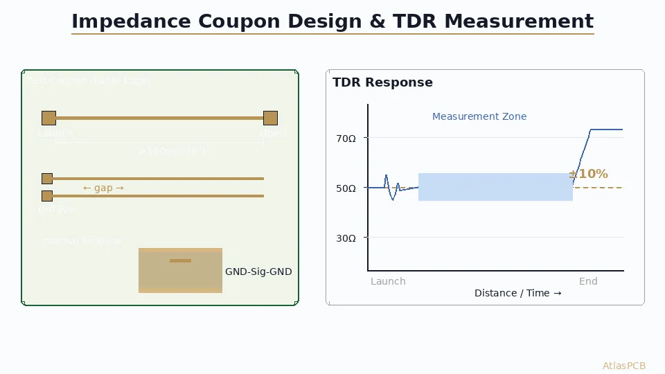
- TCK requires controlled impedance if chain length > 20 cm or clock > 20 MHz
- Add series termination resistors (33Ω) on TCK and TMS near the driving source
- Pull TDI HIGH and TMS HIGH with 10kΩ resistors for safe startup state
- Provide individual pull-ups on each device’s TRST if used
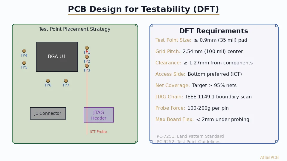
Test Point Strategy
For maximum fault coverage, combine boundary scan with selective physical access:
- Power rail test points: At least one test point per voltage rail for power-up verification
- Non-JTAG net access: Provide test pads for signals that only connect between non-JTAG devices
- Analog signals: Boundary scan cannot test analog — these need probe access
- Clock outputs: Add test points on critical clocks for frequency verification
Test point specifications:
- Minimum pad size: 0.9 mm diameter (for flying probe)
- Minimum pitch: 2.0 mm center-to-center (for fixture probes)
- Grid alignment: 2.54 mm (100 mil) grid preferred for bed-of-nails
Fault Coverage Analysis
Coverage Calculation
Boundary scan fault coverage = (Testable connections / Total connections) × 100%
Typical coverage levels:
| Board Category | JTAG Device % | Structural Coverage | Notes |
|---|---|---|---|
| FPGA-heavy (server) | >90% | 92-98% | Excellent, most nets between JTAG devices |
| Processor board | 60-80% | 75-85% | Good, add test points for analog/power |
| Mixed analog-digital | 30-50% | 40-55% | Supplement with ICT/flying probe |
| Analog-dominant | <20% | <25% | Boundary scan alone insufficient |
Combined Test Strategy
The industry best practice is a layered test approach:
- Boundary scan (seconds): Verify all BGA/CSP interconnects, program devices
- ICT or flying probe (seconds to minutes): Test passive values, analog circuits, power
- Functional test (variable): System-level verification, boot test, communication checks
This combination achieves >99% fault coverage while keeping test time under 2 minutes for most assemblies.
Economic Justification
Cost of Not Testing
For a board with 2,000 solder joints:
- Industry average solder defect rate: 20-50 DPMO (defects per million opportunities)
- Expected defects per board: 0.04-0.1
- Without testing: 4-10% of boards ship with latent defects
- Field failure cost: 10-100× the cost of factory detection
Boundary Scan ROI
- Equipment cost: Software license ($5,000-$50,000/year) + JTAG controller hardware ($2,000-$15,000)
- Per-board test cost: $0.02-$0.10 (electricity + depreciation)
- Test time: 2-10 seconds per board
- Break-even: Typically 500-2,000 boards depending on assembly complexity
Compare with:
- ICT fixture: $10,000-$50,000 per board design + $0.05/board test cost
- Flying probe: No fixture, but $0.50-$2.00/board and 1-5 minutes per board
Advanced Boundary Scan Standards
IEEE 1149.6 (AC-Coupled Boundary Scan)
Standard 1149.1 cannot test AC-coupled connections (capacitor in series on differential links like PCIe, USB). IEEE 1149.6 extends boundary scan to test differential pairs with coupling capacitors by using edge-sensitive test logic.
IEEE 1149.7 (Compact JTAG)
Reduces the TAP interface from 4/5 wires to 2 wires (TMSC and TCKC), enabling:
- Fewer pins dedicated to test on space-constrained packages
- Star topology (not just daisy chain) for faster access to individual devices
- Zero-bit bypass for reduced scan chain length
IEEE 1500 (Embedded Core Test)
Extends the boundary scan concept inside SoCs, wrapping IP cores with test wrappers for internal interconnect testing between embedded modules.
Common Pitfalls and Solutions
Pitfall 1: Missing Pull-Resistors
Without proper pull-ups on TMS and TDI, the JTAG chain can be in an undefined state at power-up, potentially causing device lock-up or bus contention.
Solution: 10kΩ pull-up on TMS and TDI to VCC, pull-down on TCK if required by any device in the chain.
Pitfall 2: Clock Integrity on Long Chains
TCK distributed as a star from the JTAG connector can have significant skew between devices if trace lengths vary widely.
Solution: Match TCK trace lengths to within 10% of the longest trace, or use a clock buffer for chains longer than 30 cm total.
Pitfall 3: Mixed Voltage Chains
When devices in the chain operate at different I/O voltages (1.8V, 2.5V, 3.3V), TDI/TDO level translation is needed.
Solution: Use voltage-tolerant I/O or add level translators between voltage domains in the chain. Group same-voltage devices together to minimize translations.
Pitfall 4: JTAG Used Only for Debug, Not Test
Many designs include a JTAG header for debug during development but don’t optimize the chain for manufacturing test coverage.
Solution: At schematic stage, plan the JTAG chain order and identify cluster-testable non-JTAG components. Include boundary scan as a requirement in DFT reviews.
Further Reading
- PCB Electrical Testing: Flying Probe vs. Fixture
- PCB EMI Shielding and Via Fencing
- BGA X-Ray Void Analysis and IPC-7095 Inspection
- PCB Test Coupon Design and IPC Standards
Design It Right, Test It Right
AtlasPCB manufactures boards with IPC Class 3 workmanship and supports DFT-optimized designs with tight pad tolerances for BGA escape routing and controlled impedance JTAG signal routing. Whether you need prototypes or production volumes, our engineering review catches testability gaps before fabrication.
About AtlasPCB — We specialize in complex PCB manufacturing for HDI, RF, and high-reliability applications. Explore our HDI PCB manufacturing capabilities . Every order includes free engineering review. Get your quote.
Reviewed by AtlasPCB Engineering Team — IPC-certified manufacturing specialists with 15+ years of production experience in HDI, RF, and high-reliability PCB fabrication. Content based on factory floor data and real customer design reviews.
Frequently Asked Questions
What faults can boundary scan detect on a PCB assembly?
How do I add boundary scan capability to my PCB design?
Is boundary scan better than flying probe or ICT testing?
- boundary scan
- JTAG
- IEEE 1149.1
- PCB testing
- DFT
- BGA testing
- interconnect test
- flying probe
- assembly verification
- fault coverage