· Thomas Webb · Engineering · 7 min read
Thermal Management PCB Design for AI Accelerator
Design guide for PCBs carrying AI GPUs and ASICs with 300-700W TDP. Covers thermal via arrays, power delivery network design, material selection for high-temperature operation, and heatsink interface optimization.
Quick Answer
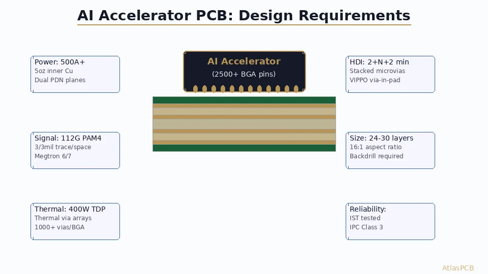
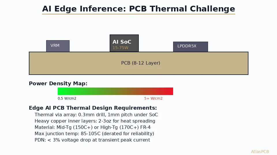
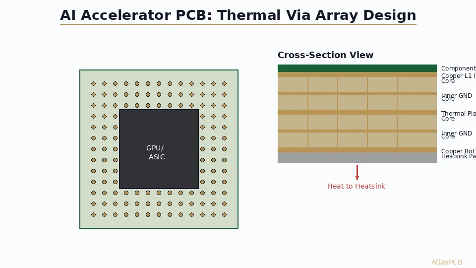
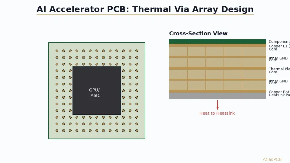
AI accelerator PCBs with 300-700W TDP require thermal via arrays (0.3mm diameter, 1.0mm pitch) under the die, 2oz+ copper on internal planes for lateral heat spreading, high-Tg materials (Tg 170C+), and optimized PDN with less than 3% voltage droop at transient loads.
The Thermal Challenge: 700W in a 50mm Package
Modern AI accelerators push 300-700W through a single BGA package mounted on a PCB. The board must simultaneously:
- Conduct heat away from the die (thermal via arrays to bottom heatsink)
- Deliver 500-800A at sub-1V to the core (power delivery network)
- Route 5,000+ high-speed signals at 112G PAM4 (signal integrity)
- Survive 5-10 years of thermal cycling (125C junction, 40C ambient)
These requirements conflict — thicker copper improves thermal/power performance but degrades signal integrity. This guide covers how to balance them.
Thermal Via Array Design
Geometry and Placement
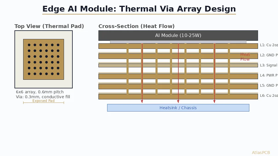
For a GPU/ASIC with exposed thermal pad:
| Parameter | Recommended | Notes |
|---|---|---|
| Via diameter | 0.3mm (12 mil) | Balances thermal conductance vs routing space |
| Via pitch | 1.0mm (40 mil) | Matches typical BGA ball pitch |
| Copper fill | Filled + planarized | Mandatory for BGA soldering |
| Pattern | Grid array under thermal pad | Cover 80%+ of exposed pad area |
| Aspect ratio | Keep below 8:1 | Ensures reliable plating fill |
Thermal Resistance Calculation
Single via thermal resistance:
- Via diameter: 0.3mm
- Board thickness: 2.4mm (typical for 16L+ server board)
- Copper wall thickness: 25 um (1 mil)
- Thermal resistance per via: approximately 70-90 C/W
For 500W die with 400 vias:
- Parallel resistance: 90/400 = 0.225 C/W
- Temperature delta (via contribution): 500W x 0.225 = 112C
This is too high. Supplementary thermal paths are essential:
- Bottom-side heatsink with thermal interface material (TIM)
- Internal copper planes for lateral heat spreading
- Thicker via plating (35-50 um) reduces per-via resistance to 50-60 C/W
HIGH-POWER PCB DESIGN
Up to 30 Layers with 5oz Copper
AtlasPCB fabricates AI server boards with filled thermal vias, heavy copper planes, and via-in-pad for BGA breakout. Min drill 0.15mm mechanical, 0.075mm laser.
Get AI Board Quote ›
Power Delivery Network (PDN) for 500A+ Loads
The Problem: Transient Response
An AI accelerator switching between idle (100W) and compute (700W) in microseconds demands:
- Less than 3% voltage droop (at 0.85V core = max 25mV droop)
- Sub-nanosecond current delivery from decoupling caps
- Ultra-low loop inductance (< 50 pH for bulk capacitor loops)
PCB PDN Design Rules
Copper weight allocation:
| Layer Function | Minimum Copper | Purpose |
|---|---|---|
| Top signal + BGA | 1oz (35 um) | Signal routing, BGA pads |
| Power planes (VCore) | 2oz (70 um) | Low-resistance power distribution |
| Ground planes | 2oz (70 um) | Return current, thermal spreading |
| Inner signal | 1oz (35 um) | High-speed routing |
| Bottom (heatsink side) | 2oz (70 um) | Thermal pad, VRM connection |
Via farm for power:
- VRM output to GPU: Use 100+ power vias (0.3mm) in parallel
- Each 0.3mm via with 25 um wall at 2.4mm length: approximately 0.5 mohm
- 100 vias in parallel: 5 uohm contribution (acceptable)
- Ground return needs equal via count
Decoupling Strategy
| Capacitor Type | Location | Purpose |
|---|---|---|
| MLCC 100nF (0201) | Under BGA, via-in-pad | High-frequency transients (>100 MHz) |
| MLCC 10uF (0402) | BGA periphery, top side | Mid-frequency (1-100 MHz) |
| Polymer 470uF | Near VRM output | Bulk energy storage (< 1 MHz) |
| VRM output caps | At VRM | Voltage regulation loop stability |
Critical: Via-in-pad for decoupling caps under BGA
Caps placed under the BGA (bottom side or in BGA field) need via-in-pad connections to power/ground planes. These vias must be:
- Filled and planarized (same as thermal vias)
- Connected to the nearest power/ground plane (not routed to distant planes)
- Placed within 2mm of the BGA power ball they serve
HDI CAPABILITY
Via-in-Pad with Copper Fill — Standard Process
We process filled and planarized vias as a standard offering. Stacked microvias up to 5+N+5 for high-density BGA breakout.
View HDI Services ›Material Selection for AI Boards
Thermal Cycling Drives Material Choice
A GPU running at 95C junction temperature with fan cycling creates thermal excursions of 60-80C every few minutes. Over 5 years, the PCB sees 100,000+ thermal cycles. This drives material requirements:
| Property | Requirement | Reason |
|---|---|---|
| Tg | 170C+ (180C preferred) | Prevents CTE jump below operating temperature |
| Td (decomposition) | 340C+ | Solder reflow safety margin |
| CTE z-axis (below Tg) | < 50 ppm/C | Minimizes via barrel stress |
| CAF resistance | High | 0.85V core with 3mil spacing demands CAF-free operation |
| Dk consistency | Moderate | 112G channels need Dk +/-0.05 stability |
Recommended Materials by Tier
Tier 1: High-performance (data center, HPC)
- Panasonic Megtron 6 (R-5775K): Dk 3.71, Df 0.004, Tg 200C
- Isola I-Speed: Dk 3.6, Df 0.004, Tg 200C
- Nelco N7000-2 HT: Dk 3.6, Df 0.005, Tg 200C
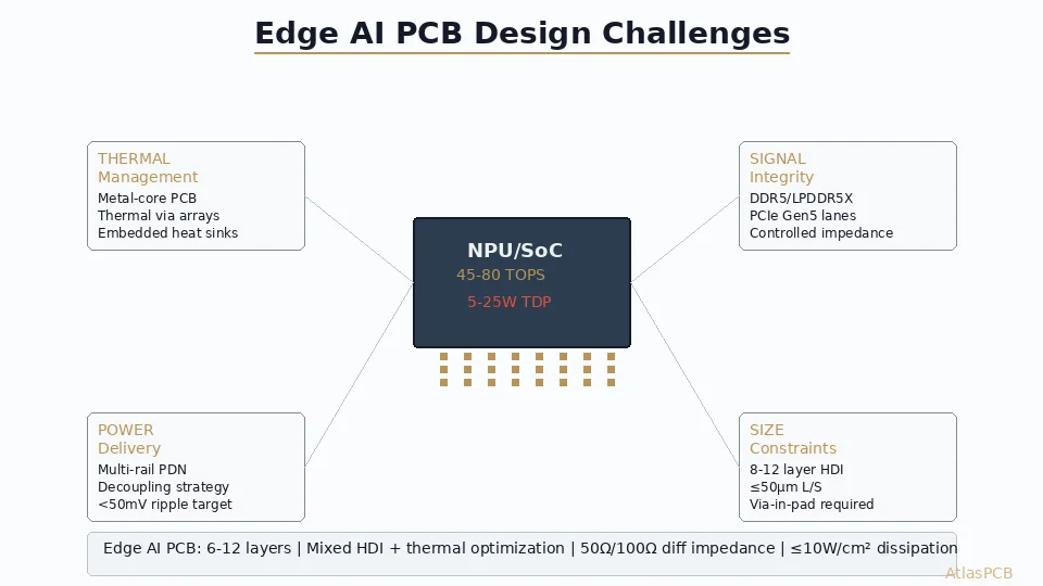
Tier 2: Mid-range (edge AI, inference servers)
- Isola 370HR: Dk 4.04, Df 0.009, Tg 180C
- Shengyi S1000-2M: Dk 4.0, Df 0.008, Tg 175C
- TUC TU-872 SLK: Dk 3.9, Df 0.008, Tg 200C
Tier 3: Budget (development boards, eval kits)
- High-Tg FR-4 (Tg 170): Dk 4.2-4.5, Df 0.015-0.020
- Adequate for prototypes where thermal cycling is limited
- Not suitable for production data center deployments
Thermal Conductivity Limits of FR-4
Even premium FR-4-based laminates conduct only 0.3-0.4 W/mK (vs copper at 400 W/mK). The board is fundamentally a thermal insulator. Heat removal strategies must rely on:
- Copper (planes and vias) for thermal conduction
- Thermal interface materials connecting to external heatsinks
- Forced airflow over board surface
For extreme cases (700W+), consider:
- Metal-core PCB for the VRM section (aluminum or copper substrate)
- Embedded copper coin under the die (provides direct thermal path)
- Thermal paste-filled through-holes (experimental, some shops offer this)
MATERIAL SELECTION
Megtron 6, I-Speed, 370HR — All In Stock
We stock high-performance laminates for AI server boards. Get material-specific pricing when you upload your design.
Compare Material Options ›Stackup Architecture: Balancing All Requirements
A typical 16-layer AI accelerator board stackup:
L1  — Top signal (BGA breakout, high-speed) — 1oz
     Prepreg 1080x2 (3.5 mil)
L2  — GND (reference for L1 impedance) — 2oz
     Core (5 mil)
L3  — Signal (inner routing) — 1oz
     Prepreg 1080x1 (3.5 mil)
L4  — VCore power — 2oz
     Core (4 mil)
L5  — GND — 2oz
     Prepreg 2116x1 (4.5 mil)
L6  — Signal — 1oz
     Core (4 mil)
L7  — GND — 2oz
     Prepreg 1080x1 (3.5 mil)
L8  — Signal — 1oz
     Core (4 mil)
L9  — Signal — 1oz
     Prepreg 1080x1 (3.5 mil)
L10 — GND — 2oz
     Core (4 mil)
L11 — Signal — 1oz
     Prepreg 2116x1 (4.5 mil)
L12 — GND — 2oz
     Core (4 mil)
L13 — VCore power — 2oz
     Prepreg 1080x1 (3.5 mil)
L14 — Signal (inner routing) — 1oz
     Core (5 mil)
L15 — GND (reference for L16 impedance) — 2oz
     Prepreg 1080x2 (3.5 mil)
L16 — Bottom signal (decap, VRM routing) — 1oz
Key design choices:
- Power planes (L4, L13) sandwiched between ground planes for low-inductance PDN
- 2oz on all GND/PWR planes for thermal and DC resistance
- Symmetric construction for warp-free assembly
- Total thickness approximately 2.4mm (standard for server boards)
Reliability: Surviving 5 Years at 125C Junction
Via Reliability Under Thermal Stress
The most failure-prone element is the plated through-hole via. At 16+ layers and 2.4mm board thickness:
- Aspect ratio: 2.4mm / 0.3mm = 8:1 (at our process limit)
- Each thermal cycle stresses the copper barrel
- CTE mismatch between copper (17 ppm/C) and FR-4 z-axis (50-70 ppm/C) creates tensile stress
Mitigation:
- Use IPC Class 3 copper plating thickness (minimum 25 um average, 20 um minimum)
- Specify IST (Interconnect Stress Test) qualification to 1000 cycles
- Consider via-in-pad fills with conductive paste for additional thermal path
- Backdrilling unused via stubs (also improves signal integrity at 56+ Gbps)
AtlasPCB performs IST and thermal cycling qualification per IPC-TM-650 for all server-class builds.
ATLASPCB
Building AI Hardware? Let's Talk Stackup.
We fabricate boards for GPU/ASIC cards with thermal via arrays, 2-5oz copper, backdrilling, and via-in-pad. Upload your design for engineering review.
Upload AI Board Design ›
Related Reading:
About AtlasPCB — We specialize in complex PCB manufacturing for HDI, RF, and high-reliability applications. Explore our aluminum and metal-core PCB services . Every order includes free engineering review. Get your quote.
Reviewed by AtlasPCB Engineering Team — IPC-certified manufacturing specialists with 15+ years of production experience in HDI, RF, and high-reliability PCB fabrication. Content based on factory floor data and real customer design reviews.
Frequently Asked Questions
How many thermal vias do I need under a GPU package?
Should thermal vias be filled or capped?
What copper weight is needed for AI PCB power planes?
Does high-Tg material help with thermal performance?
- ai-hardware
- thermal-management
- pcb-design
- power-delivery