· Thomas Webb · Engineering · 7 min read
PCB Requirements for AI Accelerator Hardware
Designing PCBs for AI accelerators (GPUs, TPUs, custom ASICs) demands extreme specifications: 20-30 layers, 500A+ current delivery, 3/3mil routing, and advanced thermal management. Here's what your fabricator needs to deliver.
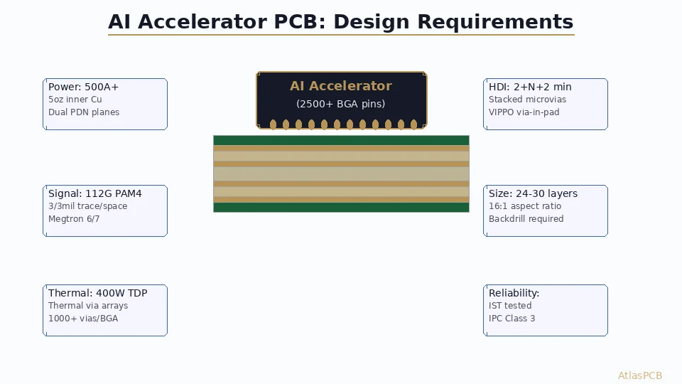
Quick Answer
AI accelerator PCBs require 20-30 layer builds with 2+N+2 or higher HDI structure, 3-5oz copper on power planes for 500A+ delivery, low-loss laminates (Megtron 6/7) for 112G PAM4 signaling, thermal via arrays (1000+ vias per BGA footprint) for 400W+ TDP dissipation, and strict impedance control with backdrilling for 16:1 aspect ratio vias. These boards represent the most demanding specifications in commercial PCB manufacturing—combining high layer count, fine-pitch HDI, heavy copper, and premium materials in a single design.
The Most Demanding PCBs in Commercial Electronics
AI accelerator hardware represents the convergence of every challenging PCB specification simultaneously: high layer count, HDI microvia structures, heavy copper power delivery, ultra-low-loss materials, extreme thermal management, and tight impedance control. A single AI training card can cost $3,000-10,000 just for the bare PCB—before any components.
This guide covers what it takes to fabricate these boards and how design choices impact manufacturability and cost.
Layer Count: Why 20-30 Layers is the Minimum
The Driving Forces
A modern AI accelerator (Nvidia B200, AMD MI300X, Google TPU v5) connects to:
- HBM3e memory: 8-12 stacks, each with 1024+ I/O at 9.6 Gbps
- PCIe Gen6 or NVLink: 112G PAM4 per lane, 16-72 lanes
- Power delivery: 0.7-0.85V core at 500-1000A
- Management/control: I2C, SPI, GPIO, thermal sensors
Routing all of this requires:
| Layer Type | Count | Purpose |
|---|---|---|
| Signal (high-speed) | 8-12 | HBM, PCIe, NVLink traces |
| Signal (low-speed) | 2-4 | Control, I2C, GPIO |
| Ground reference | 6-8 | Adjacent to every signal layer |
| Power planes | 4-8 | Multiple voltage rails at high current |
| Total | 20-30 | Typical range |
Why Not Fewer Layers?
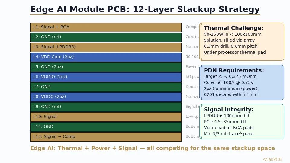
Every signal layer needs an adjacent ground reference plane for impedance control. That alone means signal + reference = 2 layers per routing tier. With 6-8 routing tiers needed for BGA escape and interconnect, plus 4-8 power planes for current density, you quickly reach 20+ layers.
Reducing layer count means wider boards (more routing space needed) or higher-density HDI (more expensive buildup). At AI-scale pin counts, 20-30 layers is actually the cost-optimized solution.
HIGH LAYER COUNT
Up to 30-Layer PCBs for AI and HPC Applications
AtlasPCB fabricates 20-30 layer boards with HDI buildup, Megtron 6 laminates, and 5oz copper power planes for AI hardware.
Get Quote for AI Board ›
Power Delivery: 500A+ at Sub-1V
The Challenge
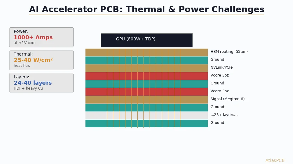
Modern AI accelerators draw 500-1000A at 0.7-0.85V. At these currents, even milliohms of PDN impedance create unacceptable voltage droop. The PCB power delivery network must achieve:
- DC resistance: < 0.5 milliohm from VRM to BGA
- AC impedance: < 1 milliohm up to 100 MHz
- Current capacity: 500A sustained, 800A+ transient
Copper Weight Requirements
Standard 1oz (35um) copper on a 50mm-wide power plane carries approximately 30A with acceptable temperature rise. To deliver 500A, you need:
| Copper Weight | Current per 50mm Width | Planes Needed (500A) |
|---|---|---|
| 1oz (35um) | ~30A | 17 planes (impossible) |
| 2oz (70um) | ~60A | 9 planes |
| 3oz (105um) | ~90A | 6 planes |
| 5oz (175um) | ~150A | 4 planes |
Practical designs use 3-5oz copper on 4-6 power/ground plane pairs, supplemented by wide copper pours on signal layers.
Via Current Distribution
The BGA-to-plane connection uses massive via arrays. A typical AI accelerator BGA has:
- 300-500 power pins
- 300-500 ground pins
- Each via carries 1-2A average
Via resistance dominates at these currents. For a 0.3mm via in a 3.5mm board:
- 0.5oz plating: ~6 milliohm per via
- 1.0oz plating: ~3 milliohm per via
1000 vias in parallel: 3-6 microhm contribution — acceptable.
Signal Integrity: 112G PAM4 on a PCB
Material Requirements
112G PAM4 signaling (the Nyquist frequency is ~28 GHz for 56 Gbaud) demands:
| Parameter | Requirement | Standard FR-4 | Megtron 6 | Megtron 7 |
|---|---|---|---|---|
| Df @ 12.5 GHz | < 0.004 | 0.020 | 0.002 | 0.001 |
| Dk variation | < +/-3% | +/-5% | +/-2% | +/-1.5% |
| Surface roughness | < 2um Rz | 6-8um | 2-3um (VLP) | 1-2um (HVLP) |
| Insertion loss (6”) | < 8 dB @ 28 GHz | >20 dB | 5-6 dB | 3-4 dB |
The copper surface roughness contribution to loss becomes dominant above 10 GHz. HVLP (Hyper Very Low Profile) copper is mandatory — standard RTF (Reversed Treat Foil) adds 3-4 dB/inch at 28 GHz.
Backdrilling: Eliminating Via Stubs
A through-via in a 24-layer board creates a stub from the signal exit point to the via end. At 28 GHz, even a 0.5mm stub creates destructive resonance. Backdrilling removes the unused stub portion:
- Target stub length: < 0.2mm (200um)
- Backdrilling accuracy: +/-3mil (AtlasPCB specification)
- Required on: all high-speed signal vias not on outer layers
Without backdrilling, via stubs create notch filters that kill eye diagrams above 16 GHz.
SIGNAL INTEGRITY
Low-Loss Materials + Precision Backdrilling
Megtron 6/7 laminates with HVLP copper foil and backdrilling to +/-3mil stub accuracy for 56+ Gbaud signaling.
View Signal Integrity Specs ›Thermal Management: Conducting Heat Through the PCB
Thermal Via Arrays
With 400W+ TDP concentrated in a 50x50mm die area, the PCB beneath becomes a thermal bottleneck. Thermal via arrays provide vertical heat conduction:
| Via Configuration | Thermal Conductivity (W/mK) | Typical Application |
|---|---|---|
| No thermal vias | 0.3 (FR-4 only) | Not acceptable |
| Via array (0.3mm, 1mm pitch) | 3-8 | Moderate power |
| Dense via array (0.2mm, 0.5mm pitch) | 15-25 | High power |
| Filled via array (copper-filled) | 30-50 | AI accelerator |
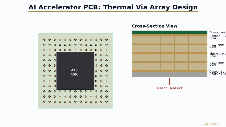
For AI boards, the area directly under the chip (die shadow) contains 1000-2000 copper-filled thermal vias in a tight grid, connected to internal copper planes that spread heat laterally to board edges and mounting hardware.
Heavy Copper as Heat Spreader
Internal 3-5oz copper planes serve dual duty: power delivery AND thermal spreading. A 5oz (175um) copper plane has thermal conductivity of 400 W/mK along its plane — 1300x better than FR-4. This makes the internal planes the primary lateral heat transport mechanism.
Manufacturing Challenges and Yield
Aspect Ratio
24-layer board, 3.5mm thickness, 0.2mm via drill: aspect ratio = 17.5:1
This exceeds standard capability. Solutions:
- Use 0.25mm minimum drill (14:1 aspect ratio) — acceptable
- Backdrilling reduces effective depth
- HDI structure avoids full-depth through-vias for many connections
Registration
At 24+ layers, layer-to-layer registration stacking becomes critical. Each layer adds +/-25um registration error. After 24 layers, total stack can reach +/-75-100um, eating into annular ring budgets.
Solution: fabricators use sequential alignment (re-registering every 4-6 layers) rather than single-stack alignment.
Yield Impact
| Board Type | Typical First-Pass Yield |
|---|---|
| 8-layer standard | 95-98% |
| 16-layer HDI | 88-93% |
| 24-layer AI (standard materials) | 80-88% |
| 24-layer AI (Megtron 6, backdrill) | 75-85% |
| 30-layer ELIC + Megtron 7 | 65-78% |
Lower yield directly impacts cost — and why AI PCBs carry premium pricing.
AI HARDWARE FABRICATION
High-Complexity PCBs for AI Infrastructure
Up to 30 layers, 5oz copper, 16:1 aspect ratio, Megtron 6. We manufacture the boards that power AI data centers.
Explore HDI Services ›Specification Summary for AI Accelerator PCBs
| Parameter | Typical Requirement | AtlasPCB Capability |
|---|---|---|
| Layer count | 20-30 | Up to 30 |
| HDI structure | 2+N+2 to 4+N+4 | Up to 5+N+5 |
| Trace/space | 3/3mil (75um) | 3/3mil minimum |
| Copper weight (inner) | 2-3oz | Up to 3oz |
| Copper weight (outer) | 2-5oz | Up to 5oz |
| Min laser drill | 0.075mm | 0.075mm |
| Aspect ratio | 14-16:1 | Up to 16:1 |
| Material | Megtron 6/7 | Megtron 6 available |
| Backdrilling | +/-3mil stub | +/-3mil accuracy |
| Board size | 300x300mm+ | Up to 1200x600mm |
| Surface finish | ENIG | ENIG, immersion silver |
| Impedance tolerance | +/-5% | +/-5% with TDR coupon |
ATLASPCB
Building AI Hardware? Let's Talk Specifications.
Upload your stackup or design files. Our engineering team has experience with high-layer-count AI boards and can provide detailed DFM feedback within 48 hours.
Upload Design Files ›
Related Reading:
- Advanced HDI PCB Stackup Design: Sequential Lamination, Any-Layer HDI, and ELIC
- High Layer Count PCB Challenges: Designing and Manufacturing 20 to 68 Layer Boards
- Signal Integrity in PCB Design: Impedance Control, Crosstalk, Via Stubs, and Return Paths
- PCB Thermal Via Design: Complete Engineering Guide
About AtlasPCB — We specialize in complex PCB manufacturing for HDI, RF, and high-reliability applications. Explore our HDI PCB manufacturing capabilities, or get an aluminum and metal-core PCB services . Every order includes free engineering review. Get your quote.
Reviewed by AtlasPCB Engineering Team — IPC-certified manufacturing specialists with 15+ years of production experience in HDI, RF, and high-reliability PCB fabrication. Content based on factory floor data and real customer design reviews.
Frequently Asked Questions
How many layers does a typical AI accelerator PCB need?
What PCB materials are needed for 112G PAM4 signaling in AI hardware?
How do you handle 400W+ thermal dissipation on a PCB?
What aspect ratio challenges exist in AI accelerator PCBs?
- AI hardware
- PCB design
- GPU
- accelerator
- HDI
- power delivery
- thermal management
- high layer count