· Thomas Webb · Engineering · 10 min read
AI-Accelerated PCB Simulation
How neural operators and ML surrogate models are replacing traditional FEM/FDTD simulation for PCB signal integrity, power integrity, and thermal analysis — delivering 100-1000x speedups that enable real-time design optimization.
Quick Answer
Machine learning surrogate models — particularly physics-informed neural operators (Fourier Neural Operators, DeepONet) — can predict PCB electromagnetic fields, impedance profiles, and thermal distributions 100-1000x faster than traditional FEM/FDTD solvers. Trained on thousands of pre-computed simulation results across geometry variations, these models enable real-time parameter sweeps and design-space exploration that would take days with conventional tools. The tradeoff: 2-5% accuracy loss versus full-physics solvers, requiring validation runs on final designs.
The Problem: Simulation Bottleneck in PCB Design
Every experienced PCB design engineer knows the frustration. You have completed your initial layout, set up impedance-controlled routing, and placed decoupling capacitors based on PDN analysis guidelines. But before committing to fabrication, you need to verify: Does the via transition from layer 3 to layer 7 maintain impedance continuity at 28 GHz? Will the power delivery network provide less than 5% voltage ripple under transient load? What is the thermal gradient across the board under maximum operating conditions?
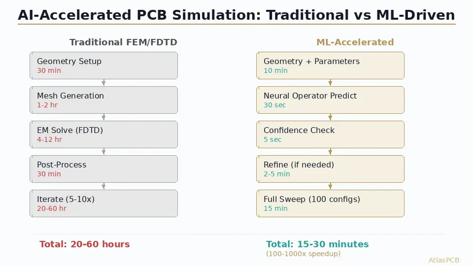
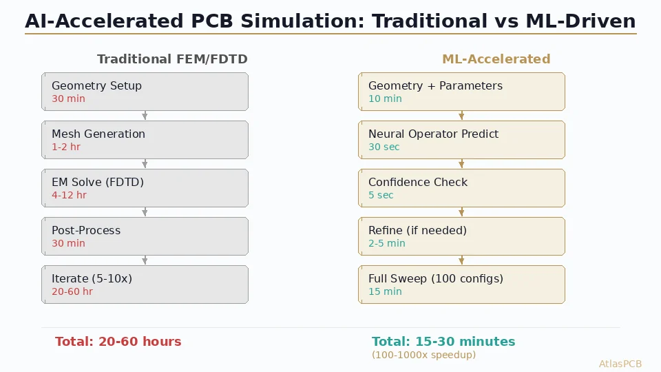
Each of these questions traditionally requires a full electromagnetic or thermal simulation. Setting up the geometry and boundary conditions takes 30-60 minutes. Mesh generation runs 1-2 hours for a complex via structure. The actual solve — whether finite element method for thermal, or finite-difference time-domain for EM — consumes 4-12 hours per configuration. Post-processing and interpretation adds another 30-60 minutes. And critically, you rarely run just one simulation. Design optimization requires sweeping parameters: what if I increase the anti-pad by 2 mil? What if I add a ground via here? What if I change the dielectric thickness by 0.5 mil?
A typical SI verification campaign involves 50-200 simulation runs across via geometries, stackup variations, and routing configurations. At 4-8 hours per run, the total simulation campaign takes 1-3 weeks of wall-clock time — often longer than the physical fabrication lead time for prototypes. This creates an absurd situation where engineers either skip simulations they should run (accepting risk) or wait weeks for verification that could have caught a design error in day one.
HIGH-SPEED DESIGN
Designing for 25+ Gbps Data Rates?
AtlasPCB manufactures impedance-controlled boards with +/-5% tolerance, backdrilling accuracy to +/-3mil, and material options from standard FR-4 to Megtron 6 for your high-speed designs.
Upload High-Speed Design ›
How ML Surrogate Models Work for PCB Applications
The core idea behind ML-accelerated simulation is straightforward: instead of solving Maxwell’s equations or heat transfer equations from scratch every time, train a neural network to predict the solution given input parameters. The network learns the mapping from geometry and material parameters to field distributions, S-parameters, impedance profiles, or temperature maps by studying thousands of pre-computed full-physics solutions.
The most promising architecture for PCB simulation applications is the neural operator family — specifically Fourier Neural Operators (FNO) and DeepONet. Unlike standard neural networks that learn point-to-point mappings, neural operators learn the underlying physics operator itself, enabling predictions for geometries and boundary conditions not seen during training (within the parameter space, not wildly different topologies). For PCB applications, this means training on via structures spanning 0.2-0.4mm diameter, 0.5-3.0mm length, 0.1-0.5mm anti-pad, and 2.5-4.5 dielectric constant produces a model that predicts S-parameters for any configuration within those ranges — including the infinite number of intermediate configurations never explicitly simulated during training.
The training process requires a one-time investment: generate 500-5000 full-physics simulations spanning the design parameter space using traditional FEM/FDTD tools. For a standard differential via pair with 8 parameters (via diameter, pad size, anti-pad, stub length, via spacing, dielectric constant, loss tangent, frequency range), 1000-2000 training samples typically achieve 97%+ accuracy on held-out test configurations. This training dataset takes 2-4 weeks to generate on a cluster but creates a model that predicts new configurations in milliseconds for years of subsequent use.
Real Applications in 2026: What’s Working Today
The theoretical promise of ML-accelerated simulation has translated into production-ready tools over the past 18 months. Cadence Clarity ML integrates neural-network surrogate models directly into the Sigrity SI/PI workflow, allowing engineers to sweep via configurations in real time — what previously required overnight batch runs now produces impedance predictions as fast as the designer can modify parameters. Internal benchmarks report 500-1000x speedup for parameter sweeps with less than 2% deviation from full FDTD results.
Ansys HFSS has incorporated ML-enhanced adaptive meshing that identifies which regions of the geometry require fine mesh resolution based on patterns learned from thousands of prior simulations. Rather than uniformly meshing the entire domain (wasteful for PCB structures where only via transitions and trace discontinuities need high resolution), the ML-guided mesher allocates resources efficiently, reducing solve time by 5-10x while maintaining accuracy. This is a more conservative but immediately deployable application of ML — it does not replace the physics solver but makes it dramatically faster by reducing the computational work required.
For thermal simulation, ML models trained on parameterized via arrays and copper pour geometries predict steady-state temperature distributions with sufficient accuracy for design-stage decisions. A thermal model trained on 2000 configurations of via array pitch, copper fill percentage, board thickness, and power dissipation can predict peak junction temperature within 2-3C of full finite-element thermal analysis — adequate for determining whether your thermal via array needs 20 or 30 vias, even if the final sign-off still uses the full solver.
THERMAL MANAGEMENT
Thermal Via Arrays and Heavy Copper for Power Dissipation
From thermal via arrays with 0.3mm pitch to 5oz copper planes for power electronics, AtlasPCB fabricates boards designed to move heat efficiently from component to heat sink.
Get Thermal Design Quote ›Practical Workflow: Integrating ML into Your Design Process
The optimal integration of ML simulation tools follows a three-tier approach that preserves rigor while capturing the speed benefits:
Tier 1 — Exploration (ML only): During initial design, use ML surrogate models for rapid what-if analysis. Sweep stackup configurations, evaluate via geometries, compare routing strategies. Run hundreds of configurations per hour. Accept 95-98% accuracy as sufficient for directional decisions. This phase replaces the “engineering intuition” step where designers previously relied on rules-of-thumb because full simulation was too expensive.
Tier 2 — Optimization (ML-guided): Once the design space is narrowed to 5-10 candidate configurations, use ML predictions to guide gradient-based or evolutionary optimization. Find the optimal anti-pad size that minimizes impedance discontinuity. Determine the minimum number of decoupling capacitors that meets PDN impedance targets. The ML model provides the objective function that optimization algorithms evaluate thousands of times — impractical with full-physics solvers, trivial with millisecond ML predictions.
Tier 3 — Validation (Full physics): Run 3-5 full FEM/FDTD simulations on the final optimized design to confirm ML predictions and generate documentation-quality results. These final runs provide the traceable, physics-based verification required for design reviews, customer documentation, and regulatory compliance. The 4-8 hours per run is acceptable at this stage because you are running them only once on a design you are confident about, rather than speculatively on hundreds of configurations.
This workflow reduces total simulation time from 2-3 weeks to 2-3 days while increasing design space coverage by 10-100x. Engineers explore more options, find better solutions, and validate with higher confidence — the rare situation where speed and quality both improve.
Limitations and When ML Falls Short
ML simulation acceleration is not a universal replacement for physics-based solvers, and understanding the failure modes prevents expensive mistakes.
Out-of-distribution predictions are the primary risk. A model trained on FR-4 geometries (Dk 3.5-4.5) cannot reliably predict behavior on Rogers 4350B (Dk 3.48 but fundamentally different loss mechanisms) or PTFE materials (Dk 2.1 with different frequency-dependent dispersion). The model has learned FR-4 physics — applying it to a different material system produces confident but wrong predictions. Always verify that your design parameters fall within the training distribution of your ML model.
Resonant structures and near-field coupling present challenges because these phenomena are highly sensitive to exact geometry. A 0.5 mil change in via spacing might produce negligible impedance change in most configurations but trigger a resonance at a specific combination of length, spacing, and frequency. ML models may smooth over these sharp features if the training data did not adequately sample the resonance boundaries. For designs operating near known resonance conditions (via arrays at frequencies where array periodicity creates stopbands), full-physics simulation remains necessary.
Novel topologies — geometries that do not resemble anything in the training set — produce unreliable predictions. If you invent a new via structure (perhaps a coaxial via with integrated return path), no pre-trained model will predict its behavior accurately until specifically trained on that geometry family. This is where ML’s “fast follower” nature becomes apparent: it accelerates iteration on known geometry families but does not eliminate the need for first-principles simulation on genuinely new structures.
ADVANCED MATERIALS
Design Validated — Ready to Fabricate?
AtlasPCB works with Rogers, PTFE, Megtron 6, and high-Tg FR-4. Whatever material your simulation specified, we fabricate it with the tight tolerances your SI models depend on.
Get Material-Specific Quote ›The Fabrication Connection: Why Simulation Accuracy Depends on Manufacturing Precision
Even the best simulation — whether ML-accelerated or full-physics — is only as good as the fabrication process that realizes the design. A simulation predicting 50.0 ohms impedance assumes the fabricator hits exact dielectric thickness, copper width after etching, and dielectric constant at the specified resin content. Manufacturing variation introduces the reality gap between simulated and measured performance.
This is where the choice of PCB fabricator directly impacts whether your simulation results translate to physical boards. A fabricator with +/-10% thickness tolerance and +/-1 mil etch variation introduces impedance uncertainty of 5-8% regardless of your simulation accuracy. A fabricator controlling thickness to +/-5% and etch to +/-0.5 mil reduces this to 2-3%. The effort you invest in simulation optimization is wasted if manufacturing variation exceeds your design margins.
The practical implication: when your ML-guided optimization determines that your design needs a specific trace width within +/-0.3 mil to maintain 50 +/-2.5 ohms impedance, verify that your chosen fabricator can actually hold that tolerance. Request process capability data (Cpk values) for trace width control on similar layer configurations. The best simulation workflow in the world cannot overcome a fabrication process that cannot reproduce the simulated geometry.
ATLASPCB
Tight Tolerances That Match Your Simulation Precision
+/-5% impedance tolerance, +/-0.5mil trace width control, and TDR verification on every impedance-controlled panel. Your simulated performance becomes measured performance.
Get Precision Quote ›
Related Reading:
About AtlasPCB — We specialize in complex PCB manufacturing for HDI, RF, and high-reliability applications. Explore our impedance-controlled PCB manufacturing, or get an aluminum and metal-core PCB services . Every order includes free engineering review. Get your quote.
Reviewed by AtlasPCB Engineering Team — IPC-certified manufacturing specialists with 15+ years of production experience in HDI, RF, and high-reliability PCB fabrication. Content based on factory floor data and real customer design reviews.
Frequently Asked Questions
How accurate are ML-based PCB simulations compared to traditional solvers?
What PCB simulation tasks benefit most from ML acceleration?
Do I need to train my own ML models for PCB simulation?
When should I still use traditional FEM/FDTD simulation?
What hardware is needed to run ML-accelerated PCB simulations?
- AI PCB design
- machine learning
- simulation
- signal integrity
- thermal analysis
- neural operator