· David Okafor · Engineering · 9 min read
Aerospace PCB Pricing
Detailed cost breakdown of aerospace-grade PCB fabrication to IPC-6012 Class 3/3A and AS9100 requirements. Identifies the actual cost drivers — inspection, documentation, and yield loss from coupon allocation — and provides strategies to reduce spend by 20-35% without compromising certification compliance.
Quick Answer
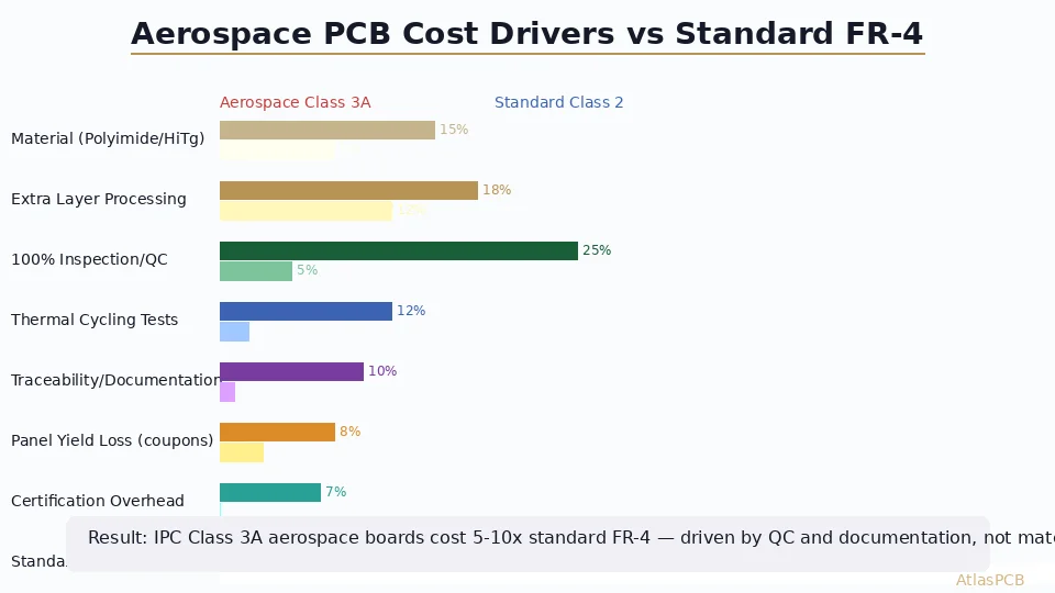
Aerospace PCBs cost 5-10x more than equivalent standard boards, but the premium is driven primarily by inspection and documentation (40-50% of the markup), not materials or extra processing. The largest cost components are 100% cross-section inspection, thermal cycling verification, per-panel traceability documentation, and yield loss from mandatory test coupon allocation. Engineers can reduce aerospace PCB costs by 20-35% through optimized coupon placement, consolidated inspection batches, and design choices that align with manufacturer process capabilities.
Quick Answer: Where Does the Aerospace Premium Go?
| Cost Category | Standard Class 2 | Aerospace Class 3A | Multiplier |
|---|---|---|---|
| Material (High-Tg/Polyimide) | $15-30/panel | $25-60/panel | 1.5-2x |
| Base Processing | $40-80/panel | $60-120/panel | 1.5x |
| Inspection and Testing | $5-10/panel | $80-200/panel | 10-20x |
| Documentation/Traceability | $2-5/panel | $30-60/panel | 10-15x |
| Coupon Yield Loss | 5% panel waste | 15-20% panel waste | 3-4x |
| Certification Overhead | Minimal | $20-40/panel | — |
| Total per panel | $70-130 | $350-700 | 5-7x |
The critical insight: material and processing — the things you might assume drive cost — account for less than 30% of the aerospace premium. Inspection, testing, and documentation consume over half the markup.
The Anatomy of Aerospace PCB Costs
Materials: The Smallest Part of the Premium
Engineers often assume the aerospace PCB cost premium comes from exotic materials. In reality, most aerospace boards use standard materials that happen to be tightly characterized and lot-controlled. A high-Tg FR-4 laminate (Isola 370HR, IT-180A) that costs $8-12 per square foot for standard production costs $12-18 for aerospace because the supplier provides full lot traceability, material certification, and qualification testing documentation with every shipment. The material itself is identical — you are paying for the paper trail.
When specifications do require specialty materials — polyimide (Dupont AP series) for extreme thermal environments, or Rogers RO4350B for RF applications in avionics — the material premium is significant ($40-80/sqft versus $8-12 for FR-4) but predictable. We run approximately 35% of our aerospace production on specialty laminates, with the remainder on qualified high-Tg FR-4 systems that meet thermal cycling requirements at lower cost.
The material decision is often the easiest optimization opportunity for cost-conscious aerospace programs. If your thermal requirement is survival to 260°C reflow (standard lead-free) with operation at -55 to +125°C, high-Tg FR-4 (Tg > 170°C, Td > 340°C) meets the requirement at one-third the cost of polyimide. Unless you are operating above 150°C continuously or require outgassing compliance for space applications, FR-4 is technically and economically appropriate.
AEROSPACE FABRICATION
IPC Class 3/3A with Full Traceability
AS9100-compliant fabrication with per-panel documentation, thermal cycling verification, and cross-section reporting.
Request Aerospace Quote ›
Inspection: The Dominant Cost Driver
The single largest cost component in aerospace PCB production is inspection — and it scales with complexity in ways that surprise procurement teams used to standard PCB pricing models.
For a standard Class 2 board, quality inspection means automated optical inspection (AOI) of outer layers plus electrical test (flying probe or fixture). Total inspection time per panel: 5-15 minutes. Cost allocation: $5-10 per panel.
For IPC-6012 Class 3A, inspection includes all of the standard testing plus: cross-section microsectioning at 3-5 locations per panel (examining plating thickness, void rate, grain structure, barrel crack propagation), TDR impedance measurement on dedicated coupons, solderability testing per J-STD-003, ionic contamination measurement per IPC-TM-650, and potentially Interconnect Stress Testing (IST) on qualification panels. Total inspection time per panel: 2-4 hours of technician time. Cost allocation: $80-200 per panel depending on complexity.
The cross-section process alone is instructive. Preparing a microsection involves mounting the sample in epoxy, grinding and polishing through multiple grit stages (220 through 1200 grit, then alumina polish), etching to reveal grain structure, and examining under 100-400x microscope with dimensional measurement. A skilled technician produces 4-6 cross-sections per hour. At 3-5 locations per panel, cross-sectioning alone consumes $40-80 of the per-panel cost.
In our aerospace production, we have invested in automated cross-section preparation equipment that reduces per-sample time by approximately 40% — but the fundamental labor intensity of microscope examination and measurement cannot be automated without compromising the judgment calls required for acceptance per IPC-A-600.
Documentation and Traceability
Every aerospace PCB must ship with a documentation package that traces the board back to specific material lots, process parameters, and inspection results. This is not simply a certificate of conformance — it is a multi-page package including:
- Material certificates with lot numbers traceable to laminate manufacturer
- Drill program revision records
- Plating bath chemistry logs during the production run
- Thermal profiling data from lamination
- All inspection results (cross-section photos, impedance data, electrical test results)
- First article inspection report (for initial qualification)
- Non-conformance reports for any deviations (even those dispositioned as acceptable)
Assembling this documentation package requires dedicated quality engineering time — typically 30-60 minutes per production batch plus 10-15 minutes per unique panel design. For small-quantity aerospace orders (5-20 panels), the documentation overhead per panel is substantial because the fixed quality engineering time is amortized across fewer units.
This is where order consolidation becomes a powerful cost optimization tool. Batching multiple purchase orders into a single production run amortizes the documentation overhead, process qualification, and first article costs across more panels — reducing per-unit documentation cost by 40-60% compared to individual small orders.
Test Coupon Allocation: Hidden Panel Waste
Every aerospace panel must include dedicated test coupons — sacrificial sections of the panel that undergo destructive testing to verify the production process. These coupons occupy real estate that could otherwise contain product boards, reducing panel utilization and directly increasing per-board material cost.
Typical coupon requirements for IPC-6012 Class 3A include:
- Impedance test coupon (if impedance-controlled): 25-40mm along panel edge
- IST coupon (4-6 locations): 30-50mm each
- Solderability test strip: 10-15mm
- Cross-section coupon strip: 15-25mm
- Thermal stress coupon: 20-30mm
Total coupon area: approximately 15-20% of usable panel area for a typical 18x24” production panel. This means a panel that would yield 12 product boards in standard production only yields 10 in aerospace production — a direct 15-20% cost increase before any other premium is applied.
Optimizing coupon placement is one of the most effective cost reduction strategies available. By collaborating with the manufacturer during design phase, coupons can be positioned to overlap with panel borders, rail areas, or breakaway tabs that would be wasted anyway. Proper placement can recover 5-10% of the panel utilization lost to coupons, saving $15-40 per panel.
COST OPTIMIZATION
Aerospace PCB Design for Manufacturability Review
We review your aerospace design for optimal panel utilization, coupon placement, and material selection — identifying 20-35% cost reduction opportunities before production.
Cost Optimization Strategies (Without Compromising Certification)
Strategy 1: Design to Manufacturer Standard Stackups
Every aerospace PCB manufacturer has qualified stackup profiles that they have characterized, tested, and documented. Using a standard qualified stackup eliminates process development NRE ($2,000-5,000 per new stackup), reduces first-article risk, and leverages existing qualification data.
Before finalizing your stackup, request the manufacturer’s standard aerospace-qualified profiles. Often a minor adjustment (changing dielectric thickness by 1-2 mils, adjusting copper weight) aligns your design with an existing qualification — saving weeks of lead time and thousands in NRE.
Strategy 2: Consolidate Orders
If your program requires multiple PCB part numbers, batch them into a single purchase order with coordinated production timing. This amortizes:
- Process qualification across multiple part numbers
- First article inspection costs
- Documentation package fixed costs
- Material incoming inspection (one material lot serves multiple designs)
Programs that order 5 different board designs individually at 20 panels each pay significantly more per panel than those ordering all 100 panels in a coordinated batch.
Strategy 3: Align Design Complexity with Actual Requirements
Not every feature on an aerospace board requires Class 3A treatment. IPC-6012 allows mixed-class callouts where specific features are held to 3A criteria while less critical areas follow Class 3 or even Class 2 acceptance levels. For example, power plane layers with 20-mil traces rarely need the same inspection scrutiny as fine-pitch signal layers.
Discuss with your manufacturer which features on your design drive inspection cost, and evaluate whether the specification can be tailored to focus Class 3A scrutiny only where reliability is genuinely critical.
Strategy 4: Material Rationalization
If your current specification calls for polyimide and your actual operating environment is -40 to +105°C with standard reflow assembly, evaluate whether high-Tg FR-4 (Tg > 170°C, Td > 340°C) meets the requirement. The material cost difference is 2-3x, and FR-4 processes more predictably (fewer lamination defects, more consistent drill quality) — which also improves yield.
Similarly, if ENIG surface finish is specified but the board does not require wire bonding or multiple reflow cycles, ENEPIG or immersion silver may be technically equivalent at lower cost.
ENGINEERING CONSULTATION
Need Help Optimizing Aerospace PCB Costs?
Our aerospace team reviews specifications against actual requirements, identifying where overspecification inflates cost without adding reliability value.
Discuss Your Project ›Typical Pricing Ranges by Board Complexity
| Board Type | Class 2 ($/board, 50pcs) | Class 3A ($/board, 50pcs) | Premium |
|---|---|---|---|
| 4-layer FR-4, standard features | $8-15 | $45-80 | 5-6x |
| 8-layer, impedance controlled | $25-50 | $150-300 | 6-7x |
| 12-layer HDI, blind/buried vias | $80-150 | $500-900 | 6-7x |
| 16-layer, Rogers hybrid RF | $150-300 | $900-1800 | 6-8x |
| Rigid-flex, 6-layer | $100-200 | $600-1200 | 6-7x |
These ranges assume standard production panel sizes (18x24”) with typical board dimensions (50-150mm per side). Very large boards, unusual form factors, or extremely tight feature tolerances push costs toward the higher end.
Summary: Controlling Aerospace PCB Spend
The aerospace PCB cost premium is real but manageable once you understand that it is driven by inspection and documentation rather than materials or processing. Engineers and procurement teams who collaborate with their manufacturer early in the design phase — sharing the end-use environment, actual reliability requirements, and volume projections — consistently achieve 20-35% lower costs than those who submit a finished design with blanket Class 3A callouts and request a quote.
The key insight: every specification decision on your drawing translates directly to inspection labor, testing time, and documentation effort at the fabricator. Precision in your requirements — specifying exactly what you need and nothing more — is the most powerful cost lever available.
ATLASPCB
Get an Optimized Aerospace PCB Quote
Upload your design and specification. We provide detailed cost breakdown showing exactly where your spend goes — plus optimization recommendations.
Request Detailed Quote ›
Reviewed by AtlasPCB Engineering Team — 15+ years in advanced PCB fabrication for RF, HDI, and rigid-flex applications.
Related Reading:
About AtlasPCB — We specialize in complex PCB manufacturing for HDI, RF, and high-reliability applications. Explore our instant online PCB quote, or get an full PCB manufacturing capabilities . Every order includes free engineering review. Get your quote.
Reviewed by AtlasPCB Engineering Team — IPC-certified manufacturing specialists with 15+ years of production experience in HDI, RF, and high-reliability PCB fabrication. Content based on factory floor data and real customer design reviews.
Frequently Asked Questions
Why do aerospace PCBs cost so much more than standard boards?
What is the cost difference between IPC Class 3 and Class 3A?
How can I reduce aerospace PCB cost without compromising reliability?
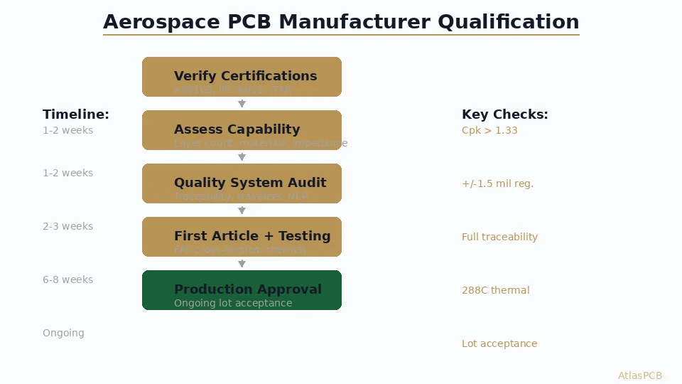
What certifications does an aerospace PCB manufacturer need?
What is the typical lead time for aerospace PCBs?
- PCB manufacturer for aerospace
- aerospace PCB cost
- IPC 6012 Class 3
- AS9100
- PCB pricing