· AtlasPCB Engineering · Engineering · 10 min read
5G Small Cell Base Station PCB: Rogers/FR-4 Hybrid Stack for Sub-6 GHz and mmWave Dual-Band Modules
A manufacturing-focused guide to PCB construction for 5G small cell base stations covering dual-band (sub-6 GHz + mmWave) designs. Details the Rogers/FR-4 hybrid stackup approach, via transition management at 28 GHz, thermal dissipation for integrated PA modules, and material selection trade-offs specific to outdoor small cell deployment conditions.
Quick Answer
5G small cell base station PCBs for dual-band operation (sub-6 GHz + 28 GHz mmWave) use a hybrid stackup with Rogers RO4350B or RO4835 on RF layers and standard high-Tg FR-4 for digital/power layers. The critical manufacturing challenges are managing CTE mismatch at material boundaries during thermal cycling (-40C to +85C outdoor deployment), maintaining via impedance continuity through layer transitions at mmWave frequencies, and integrating thermal via arrays under PA modules that dissipate 10-30W in a compact form factor.
The 5G Small Cell PCB Challenge
5G small cell base stations represent one of the most demanding PCB applications in current production: they combine RF performance requirements comparable to aerospace radar with cost constraints closer to consumer electronics, all packaged in a compact form factor that must survive outdoor environmental exposure for 10+ years.
A typical dual-band small cell module integrates sub-6 GHz massive MIMO (3.5-4.9 GHz, 64T64R) and mmWave beamforming (24.25-29.5 GHz, 256-element phased array) on a single PCB or closely integrated PCB assembly. The PCB must simultaneously achieve less than 0.5 dB insertion loss per centimeter at 28 GHz on antenna feed lines, support 10-30W PA thermal dissipation without active cooling, maintain impedance control within +/-5% across -40C to +85C temperature range, and survive 20+ years of outdoor thermal cycling without via barrel cracking or delamination.
Meeting all four requirements simultaneously — within a target PCB cost that enables deployment of millions of units — drives the hybrid stackup approach that has become the industry standard for 5G infrastructure boards.
Hybrid Stackup Architecture: Material-by-Function Assignment
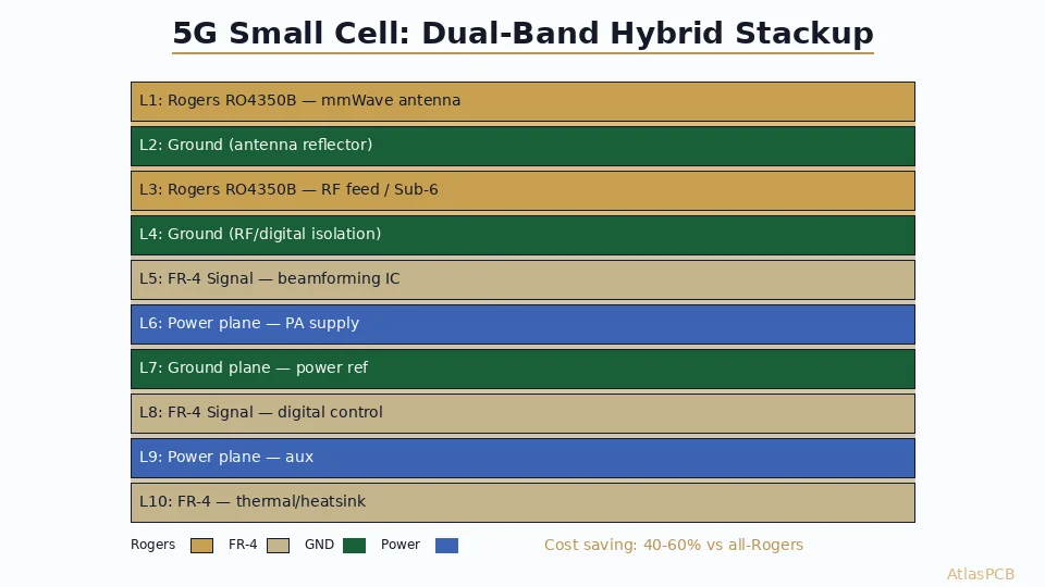
The guiding principle for 5G small cell PCB stackup design is simple: use expensive low-loss material only where RF signals actually travel, and use cost-effective FR-4 everywhere else. In practice, this means a 10-16 layer stackup with 2-4 Rogers layers sandwiched between FR-4 digital and power layers.
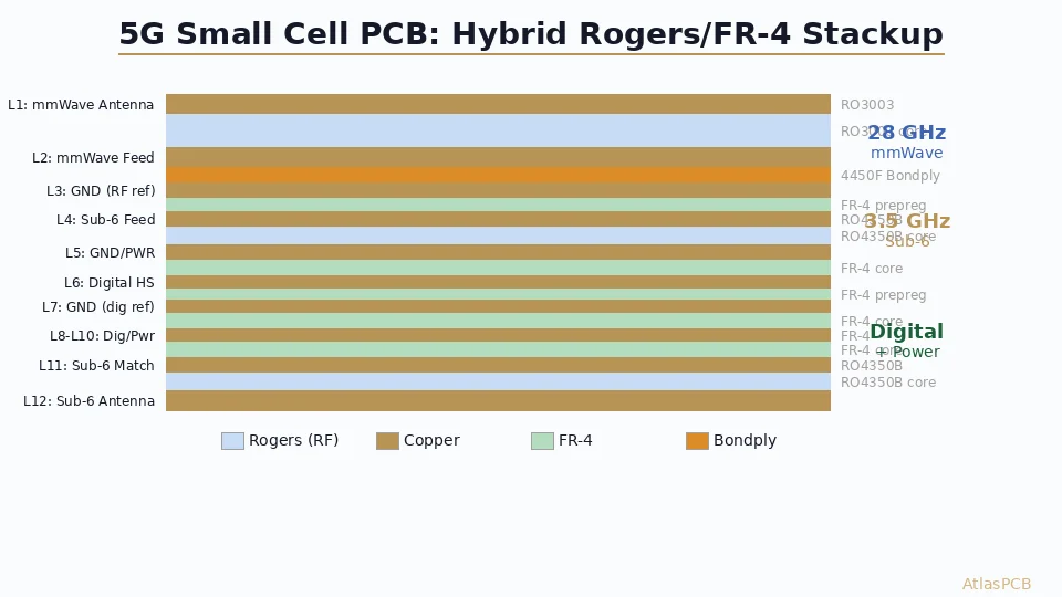
Reference Stackup: 12-Layer Dual-Band Small Cell
| Layer | Function | Material | Copper | Notes |
|---|---|---|---|---|
| L1 | mmWave antenna elements | Rogers RO3003 (0.5mm) | 0.5 oz | Patch antenna array, 28 GHz |
| L2 | mmWave feed network | Rogers RO3003 | 1 oz | Stripline feed, controlled impedance |
| L3 | Ground (RF reference) | FR-4 prepreg bond | 1 oz | Continuous ground, via stitching |
| L4 | Sub-6 GHz antenna feed | Rogers RO4350B (0.254mm) | 1 oz | 3.5 GHz feed network |
| L5 | Ground/power | FR-4 core (0.2mm) | 2 oz | PA thermal plane |
| L6 | Digital high-speed | FR-4 core (0.1mm) | 1 oz | JESD204B, PCIe to baseband |
| L7 | Ground (digital reference) | FR-4 prepreg | 1 oz | Signal integrity reference |
| L8 | Digital control/slow | FR-4 core (0.2mm) | 1 oz | SPI, I2C, GPIO |
| L9 | Power distribution | FR-4 core (0.2mm) | 2 oz | 48V input, DC-DC zones |
| L10 | Ground | FR-4 prepreg | 2 oz | Thermal via landing |
| L11 | Sub-6 GHz PA matching | Rogers RO4350B (0.254mm) | 1 oz | Output matching network |
| L12 | Sub-6 GHz antenna | Rogers RO4350B | 0.5 oz | Patch array, 3.5 GHz |
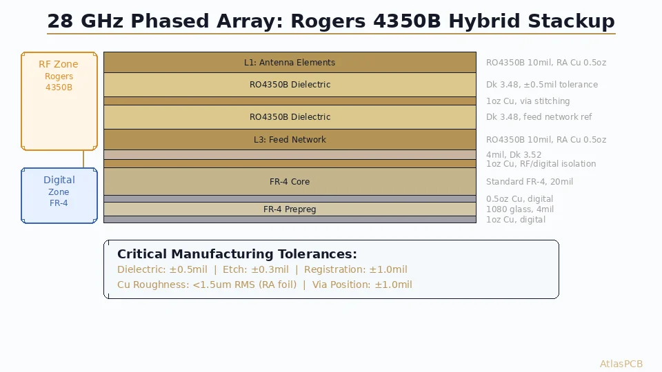
This 12-layer construction uses 4 Rogers layers (L1-L2 for mmWave, L4 and L11-L12 for sub-6 GHz) and 8 FR-4 layers for digital, power, and ground. The material cost split is approximately 55% Rogers (despite being only 33% of layers) and 45% FR-4 including prepreg — still roughly 60% cheaper than an all-Rogers construction.
The key manufacturing challenge in this stackup is the material boundary between Rogers and FR-4 layers. Standard FR-4 prepreg cannot directly bond to Rogers laminates without reliability risk during thermal cycling. We use Rogers 4450F bondply (Dk 3.52, CTE matched to RO4350B) at the Rogers-to-FR-4 interfaces, which provides both good RF performance in the transition zone and reliable adhesion across the operating temperature range.
5G RF PCB MANUFACTURING
Rogers/FR-4 Hybrid Stackups for 5G Infrastructure
Production-proven hybrid constructions from 3.5 GHz to 28 GHz. We stock Rogers RO4350B, RO3003, and 4450F bondply for consistent availability on 5G programs.

Via Strategy for mmWave Layer Transitions
At 28 GHz, a quarter wavelength in Rogers RO3003 (Dk 3.0) is approximately 1.56mm. This means via transitions between layers are electrically significant — a poorly designed via can introduce 1-2 dB of loss and create impedance discontinuities that detune the antenna feed network. The via strategy for mmWave small cell PCBs must be designed specifically for the operating frequency.
Signal Via Design for 28 GHz
The target is maintaining 50-ohm impedance through the via transition from the surface antenna layer to the internal feed network. The via impedance is controlled by the ratio of via pad diameter to antipad (clearance hole) diameter in surrounding ground planes.
For 50-ohm via impedance in Rogers RO3003 (Dk 3.0):
- Via drill: 0.15mm (laser) or 0.20mm (mechanical)
- Via pad: 0.30-0.35mm
- Antipad: 0.55-0.65mm
- Surrounding ground vias: 0.60mm pitch from signal via center
The critical manufacturing requirement is antipad registration accuracy. At 28 GHz, a 0.05mm antipad shift changes via impedance by approximately 3 ohms — enough to create a measurable reflection. This demands layer-to-layer registration within +/-1 mil (0.025mm), which is achievable on dedicated panel manufacturing but difficult to guarantee on pool service production.
Ground Via Stitching for mmWave Isolation
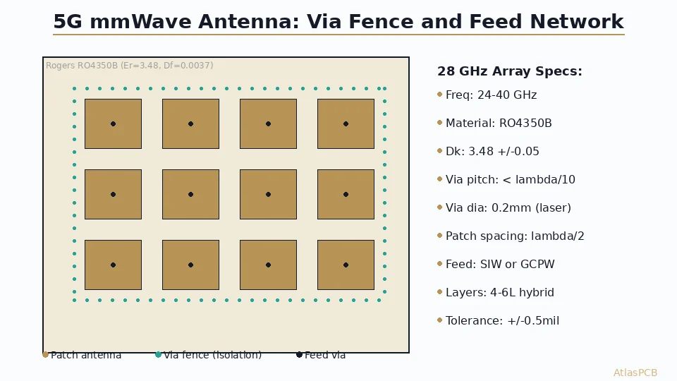
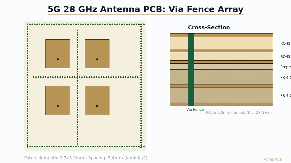
Between antenna elements and between RF channels, ground via stitching provides inter-element isolation and prevents surface wave propagation along the Rogers layer. The via spacing rule for effective shielding at frequency f is:
Via pitch less than lambda/10 in the dielectric medium.
At 28 GHz in RO3003: lambda = c / (f x sqrt(Dk)) = 6.19mm, so maximum via pitch = 0.62mm.
In practice, we use 0.5mm pitch ground via fencing around each antenna element and between RF channels. This requires dense via drilling — a 256-element phased array at 28 GHz with proper stitching may have 3000-5000 ground vias in addition to signal and power vias. Manufacturing this density reliably requires drill bit management protocols specific to high-Dk laminates (Rogers is softer than FR-4 and dulls drill bits faster).
Thermal Management: PA Module Heat Extraction
The power amplifier modules in a 5G small cell represent the dominant heat source. A typical small cell PA array dissipates:
- Sub-6 GHz (64T64R at 3.5 GHz): 4-8W per PA module, 8-16 modules = 32-128W total
- mmWave (256 elements at 28 GHz): 0.1-0.3W per element, 256 elements = 25-75W total
For compact small cells where all RF electronics are on a single PCB, the PCB itself must conduct heat from PA devices to the external enclosure. This is accomplished through thermal via arrays — dense fields of plated-through vias directly under each PA module that create a low-resistance thermal path from the device mounting pad through the PCB to a ground plane or thermal pad on the opposite side.
Thermal Via Array Design Parameters
| Parameter | Conservative | Aggressive | Manufacturing Limit |
|---|---|---|---|
| Via diameter | 0.3mm | 0.4mm | 0.15mm min (laser) |
| Via pitch | 1.0mm | 0.8mm | 0.6mm min (mechanical) |
| Via fill | Unfilled | Copper-filled | Copper-filled adds 20% cost |
| Copper in thermal plane | 2 oz | 3 oz | 5 oz max outer layers |
| Effective theta_JC (via array) | 4-6 C/W | 2-3 C/W | — |
In our facility, we have optimized the thermal via plating process to achieve greater than 80% barrel fill on 0.3mm vias, which significantly improves thermal conductivity compared to standard plated vias (typically 25-40% fill). Combined with 2oz copper on internal thermal planes, we achieve effective PCB thermal resistance of 2.5-3.5 C/W for a 20x20mm PA footprint — adequate for outdoor deployment without active cooling up to approximately 45C ambient temperature with standard heatsinking.
The manufacturing challenge is that thermal via arrays must coexist with RF signal routing without causing electromagnetic coupling. We maintain minimum 1.5mm separation between thermal via arrays and 28 GHz signal traces, with continuous ground planes between them. This spacing constraint limits how close PA modules can be placed to antenna feed networks — a trade-off that antenna designers must account for in their array layout.
THERMAL + RF CODESIGN
We Optimize Thermal Via Placement Around Your RF Layout
Our process engineers review thermal via arrays against RF isolation requirements before production. Avoid the late-stage discovery that your thermal solution couples into your antenna array.
Submit Design for Review ›Material Selection: Environmental Durability for Outdoor Deployment
Small cell base stations mount on utility poles, building facades, and street furniture with expected service life of 15-20 years. The PCB material system must survive:
- Temperature cycling: -40C to +85C, potentially 2000+ cycles over service life
- Humidity: Up to 95% RH in tropical/coastal deployments (board is sealed in enclosure but seal degradation occurs over time)
- Vibration: Wind loading creates continuous low-frequency vibration (5-50 Hz)
These environmental requirements eliminate some material choices that would otherwise be optimal for RF performance:
PTFE (RO5880, RT/duroid): Excellent RF performance (Df 0.0009 at 10 GHz) but poor dimensional stability under thermal cycling and very difficult to bond to FR-4 reliably for 2000+ cycles. Not recommended for outdoor small cell despite superior electrical properties.
Rogers RO4350B/RO4835: Thermoset hydrocarbon/ceramic with CTE close to FR-4, excellent dimensional stability, proven reliability through 2000+ thermal cycles when properly bonded. The standard choice for small cell applications up to 10 GHz.
Rogers RO3003: PTFE/ceramic with very low loss (Df 0.0013) for mmWave layers. CTE mismatch with FR-4 is larger than RO4350B, requiring careful interface engineering. Acceptable for inner layers (less thermal stress than surfaces) when proper bondply is used.
Isola Astra MT77: Ultra-low-loss (Df 0.0017 at 10 GHz) with FR-4-compatible processing. Emerging alternative to Rogers for 5G applications where the Df difference between 0.0037 (RO4350B) and 0.0017 (Astra MT77) translates to measurable system performance improvement at mmWave frequencies.
In practice, we recommend RO4350B for sub-6 GHz layers and RO3003 for mmWave layers as the production-proven combination. Manufacturers who can reliably process the RO3003/FR-4 interface with proven thermal cycling data should be preferred for mmWave small cell programs.
Manufacturing Yield and Cost Considerations
5G small cell PCBs with hybrid Rogers/FR-4 construction typically achieve 75-85% first-pass yield at experienced manufacturers. The primary yield loss mechanisms are:
Registration failure at material boundaries: Different materials have different shrinkage coefficients during lamination, which can cause layer misregistration at Rogers-to-FR-4 interfaces. This manifests as shifted antipads around signal vias — invisible to electrical testing but measurable with cross-section analysis and catastrophic for mmWave impedance control.
Delamination at bondply interfaces: If the lamination pressure or temperature profile is not correctly tuned for the specific Rogers/FR-4 combination, the bondply interface can develop micro-delaminations that propagate during thermal cycling. We run thermal stress testing (288C solder float, 6 cycles) on coupons from every production panel to catch this before shipping.
Drill quality in mixed materials: Transitioning from FR-4 to Rogers in a through-hole drill creates different chip formation characteristics. Without appropriate drill speed/feed adjustment at material transitions, the Rogers layer can develop rough hole walls that degrade plating adhesion and via reliability. Our CNC drill programs include material-aware parameter changes at each layer transition.
Cost Structure for 5G Small Cell PCBs
| Component | Percentage of Total Cost | Key Driver |
|---|---|---|
| Materials (Rogers + FR-4) | 35-45% | Rogers laminate cost dominates |
| Drilling and plating | 15-20% | Via density, especially stitching |
| Lamination (multiple cycles) | 15-20% | Number of sequential presses |
| Impedance testing | 5-8% | Per-panel TDR for every unit |
| Surface finish (ENIG) | 5-8% | Antenna pad area drives gold usage |
| Yield loss allocation | 10-15% | Assumed in unit price |
For production volumes (1000+ panels), total cost ranges from $80-150 per panel for a 12-layer hybrid stackup of the type described above (assuming 200x250mm panel size with 4 boards per panel). This translates to $20-40 per board — competitive with telecom infrastructure cost targets when amortized across the 15-year service life of the equipment.
ATLASPCB
5G Small Cell PCB Production — Prototype to Volume
Rogers/FR-4 hybrid expertise from single prototypes through 10K+ production. Material in stock, thermal cycling qualification data available. Request our 5G reference stackup library.
Get Production Quote ›
Reviewed by AtlasPCB Engineering Team — 15+ years in advanced PCB fabrication for RF, HDI, and rigid-flex applications.
Related Reading:
About AtlasPCB — We specialize in complex PCB manufacturing for HDI, RF, and high-reliability applications. Explore our RF and high-frequency PCB services, Rogers RO4350B PCB manufacturing, or get an multilayer PCB fabrication up to 30 layers . Every order includes free engineering review. Get your quote.
Reviewed by AtlasPCB Engineering Team — IPC-certified manufacturing specialists with 15+ years of production experience in HDI, RF, and high-reliability PCB fabrication. Content based on factory floor data and real customer design reviews.
Frequently Asked Questions
Why use a hybrid Rogers/FR-4 stackup instead of all-Rogers for 5G small cell PCBs?
What Rogers material is best for 5G small cell applications?
How do you manage thermal cycling in outdoor small cell PCBs?
What via design is needed for 28 GHz signal transitions in small cell PCBs?
What power dissipation challenges exist in small cell PCBs?
- 5G antenna PCB fabrication
- China RF PCB manufacturer
- Rogers 4350B stackup
- RF PCB design and manufacturing
- 5G small cell