· AtlasPCB Engineering · Engineering · 10 min read
5G Small Cell PCB Design: Dual-Band Rogers/FR-4 Hybrid Manufacturing for Sub-6 GHz and mmWave
PCB manufacturing requirements for 5G small cell antenna modules combining Sub-6 GHz and mmWave bands. Covers hybrid Rogers/FR-4 stackup design, antenna array pattern accuracy, thermal management at the board level, and fabrication tolerances that determine array performance.
Quick Answer
5G small cell PCBs combining Sub-6 GHz (3.5-3.7 GHz) and mmWave (24-28 GHz) bands require hybrid stackups with Rogers RO4350B on antenna layers and standard FR-4 on digital/power layers. Critical manufacturing parameters are etch tolerance of ±0.5 mil for mmWave patch elements, Dk variation below ±2% across the panel for consistent array phase, and CTE-matched prepreg at the Rogers/FR-4 boundary to prevent delamination under thermal cycling from power amplifier heat.
The 5G Small Cell PCB Challenge: Two Frequency Worlds on One Board
5G small cells present a unique PCB manufacturing challenge that most standard fabrication shops cannot address: combining two fundamentally different RF bands — Sub-6 GHz (typically 3.3-3.8 GHz for n77/n78) and mmWave (24.25-29.5 GHz for n257/n258/n261) — on a single PCB assembly with integrated antenna elements.
The Sub-6 GHz portions are achievable with high-quality FR-4 or mid-loss laminates. The Dk stability and loss tangent requirements at 3.5 GHz are moderate enough that careful material selection within the FR-4 family can work. But the mmWave antenna elements — patch arrays operating at 26 or 28 GHz — demand material performance that only dedicated RF laminates like Rogers RO4350B or RO3003 can provide.
The manufacturing challenge is not choosing one material over another. It is fabricating a single board that combines both materials in a controlled, reliable, and cost-effective hybrid structure.
Hybrid Stackup Architecture: Where Rogers Goes and Why
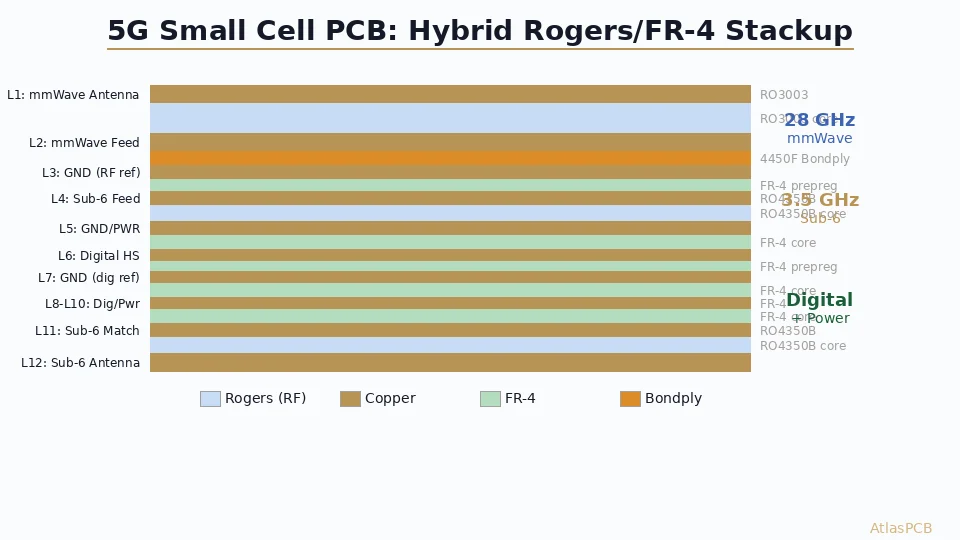
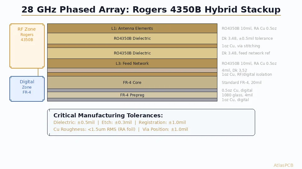
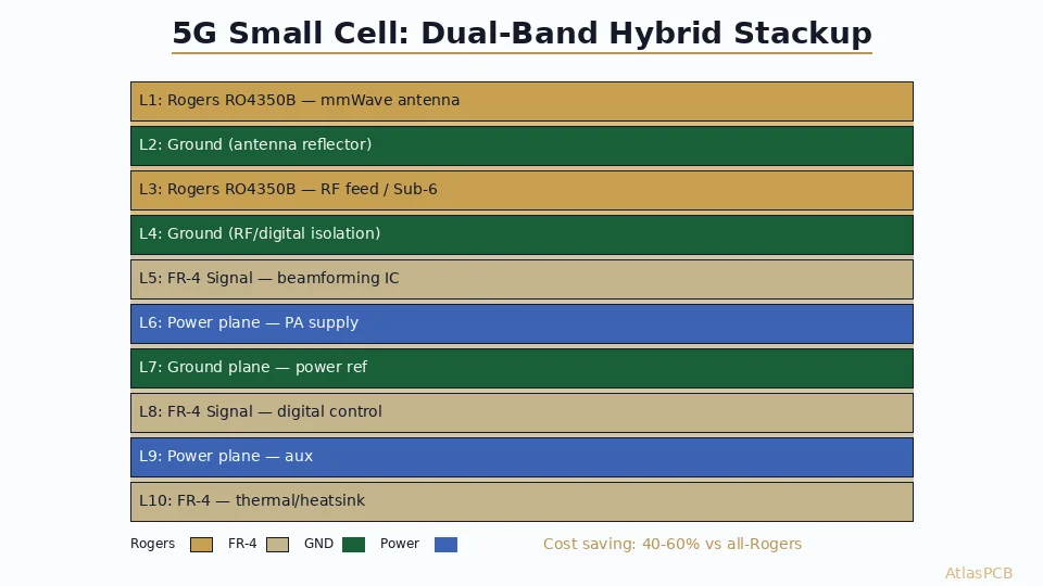
Typical 10-Layer 5G Small Cell Stackup
L1:  Rogers RO4350B (20mil) — mmWave patch antenna array
L2:  Ground plane (antenna reflector) — critical spacing to L1
L3:  Rogers RO4350B (10mil) — RF feed network / Sub-6 GHz elements
L4:  Ground plane — RF/digital isolation barrier
L5:  FR-4 signal — beamforming IC routing
L6:  Power plane — PA supply, digital VCC
L7:  Ground plane — power integrity reference
L8:  FR-4 signal — digital control, SPI/I2C, JESD204B
L9:  Power plane — auxiliary supplies
L10: FR-4 signal — thermal relief pads, heatsink interface
The Rogers layers (L1, L3) handle all RF-critical paths. The FR-4 layers (L5, L8, L10) carry digital signals and power distribution. The transition boundary between Rogers and FR-4 sections requires careful prepreg selection to manage CTE mismatch.
Why Material Placement Matters for Array Performance
At 28 GHz, a quarter wavelength in Rogers RO4350B (Dk 3.48) is approximately 1.44mm. The patch antenna element dimensions are directly tied to this wavelength — meaning any Dk variation across the panel translates to resonant frequency variation between array elements.
A Dk variation of ±3% (typical for standard FR-4) would cause ±840 MHz frequency shift at 28 GHz — completely unacceptable for a band with 400-800 MHz usable bandwidth. Rogers RO4350B with ±1.5% Dk tolerance limits this to ±420 MHz, which combined with careful etch control keeps all array elements within the operational bandwidth.
In our production, we verify Dk consistency across the panel area by measuring impedance on distributed coupons (not just corner positions). For mmWave antenna arrays, we place impedance coupons at each quadrant of the panel to ensure no positional Dk gradient exceeds specification.
5G RF PCB SPECIALIST
Hybrid Rogers/FR-4 Stackups for 5G Antenna Modules
RO4350B and RO4003C in stock. Etch tolerance ±0.5 mil for mmWave patterns. Impedance verification at distributed panel positions. 10-14 day prototype.

Critical Manufacturing Parameters for mmWave Performance
Etch Tolerance: The Make-or-Break Specification
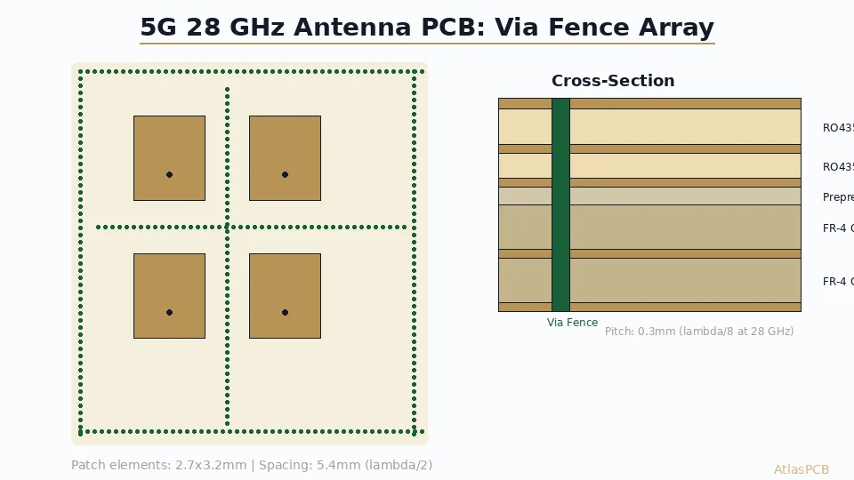
At 28 GHz, the patch antenna element dimensions are typically 2.5-3.5mm per side. The relationship between dimensional accuracy and electrical performance is approximately:
- ±1.0 mil etch error → ±500 MHz resonant frequency shift (marginal for most systems)
- ±0.5 mil etch error → ±250 MHz shift (acceptable for 400-800 MHz bandwidth)
- ±0.3 mil etch error → ±150 MHz shift (preferred for phased array consistency)
Standard PCB etching achieves ±1.0-1.5 mil. Achieving ±0.5 mil requires modified etch parameters: lower spray pressure, more uniform etchant distribution across the panel, and potentially Laser Direct Imaging (LDI) for artwork generation instead of photographic film tools which introduce their own dimensional variation.
For phased array antennas where element-to-element consistency determines beam quality, the etch uniformity across the array area matters more than absolute dimensional accuracy. An array where all elements are 0.3 mil oversized performs identically to nominal — but an array where corner elements are 0.5 mil oversized and center elements are 0.5 mil undersized has degraded beam symmetry.
Our etching process for mmWave antenna panels uses: LDI (no phototool dimensional error), reduced spray pressure for uniform etch rate across panel, and in-process measurement sampling at multiple panel positions to verify etch uniformity before completing the lot.
Lamination: Managing the Rogers/FR-4 Interface
The CTE (Coefficient of Thermal Expansion) mismatch between Rogers RO4350B (X/Y: 10-12 ppm/°C) and standard FR-4 (X/Y: 14-17 ppm/°C) creates mechanical stress at the material boundary during lamination and thermal cycling. Poor management of this interface leads to:
- Microcracking in copper traces at the boundary during thermal excursions
- Delamination between Rogers and bonding prepreg over time
- Warpage that makes array elements non-planar (degrading beam pattern)
The solution involves three process controls: using CTE-transitional prepreg at the Rogers/FR-4 boundary (materials like Rogers RO4450F bondply designed specifically for this purpose), controlling lamination ramp rates to minimize thermal stress during pressing, and maintaining symmetric copper balance across the board center to prevent differential stress.
In our 5G antenna production, we use Rogers RO4450F or Isola 185HR prepreg at hybrid boundaries. Both have intermediate CTE values that bridge the Rogers/FR-4 gap. We verify interface integrity through cross-section and thermal cycling testing on first articles.
mmWAVE FABRICATION
±0.5 mil Etch Tolerance for Antenna Patterns
LDI imaging, characterized etch uniformity, distributed panel impedance verification. We build 28 GHz antenna arrays weekly as part of our 5G production workflow.
Request mmWave Quote ›Thermal Management: PA Heat and Antenna Performance
The Thermal-RF Coupling Problem
5G small cell power amplifiers operating at Class AB for n78 typically dissipate 8-15W. This heat flows through the PCB stack, creating temperature gradients that affect antenna performance in two ways:
Dk thermal drift: Rogers RO4350B has a thermal coefficient of Dk change of approximately 50 ppm/°C. A 30°C temperature rise (typical for a 10W PA without active cooling) causes Dk to increase by 0.15%, shifting antenna resonance by approximately 40-60 MHz at 28 GHz. For Sub-6 GHz elements, this shift is proportionally smaller and usually acceptable.
Thermal expansion of array geometry: A 30°C temperature gradient across a 4x4 antenna array (typical when PA is located at one edge) causes differential expansion that changes element-to-element spacing. At 28 GHz where element spacing is approximately 5.4mm (half-wavelength), even 10μm differential expansion between elements creates measurable beam pointing error.
PCB-Level Thermal Solutions
The manufacturer’s role in thermal management extends beyond component placement — it involves stackup design and process capability:
Thermal via arrays: Dense via arrays (0.3mm drill, 0.6mm pitch) beneath PA mounting pads conduct heat from the component side to a thermal spreading plane or heatsink pad on the opposite side. For 10W dissipation, thermal resistance through the PCB stack must be below 5°C/W to keep temperature rise manageable.
Embedded copper coins: For 15W+ dissipation, thermal vias alone are insufficient. Embedded copper coins (2-3mm thick copper slugs press-fit or molded into the PCB at the PA location) reduce thermal resistance to 1-2°C/W. This requires cavity routing in the PCB and specialized lamination — adding cost and lead time but essential for high-power small cells.
Thermally-aware stackup design: Placing a thick copper ground plane (2oz minimum) between the PA layer and antenna layers serves dual purposes — thermal spreading to reduce hot-spot temperature, and electromagnetic isolation to prevent PA harmonic emissions from coupling into antenna elements.
Design-for-Manufacturing Rules Specific to 5G Antenna PCBs
Based on producing hundreds of 5G antenna panels, these DFM rules prevent the most common yield issues:
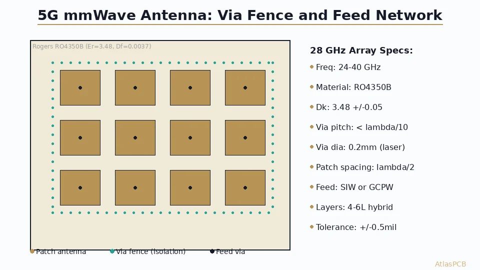
Array element clearance: Keep antenna patch elements at least 3x the substrate thickness away from any metal feature on the same layer (ground pour edges, nearby traces). Near-field coupling to adjacent copper distorts the element radiation pattern and shifts impedance.
Via-free zones beneath patches: No plated through-hole vias within the patch element footprint on any layer. Via stubs act as parasitic radiators at mmWave frequencies, creating unwanted sidelobes. Use blind vias from digital layers that terminate before reaching the antenna ground plane.
Feed network routing: RF feed lines to antenna elements should maintain consistent ground reference plane continuity. Any ground plane void (from via antipads) beneath the feed network creates impedance discontinuity. Use ground via stitching along feed network transitions.
Panel registration to antenna array: Ensure the array element positions are referenced to the panel’s primary registration features. Layer-to-layer registration tolerance of ±1.5 mil is adequate for Sub-6 GHz but may need ±1.0 mil for 28 GHz arrays where feed line alignment to elements affects phase accuracy.
DFM FOR 5G ANTENNAS
Pre-Production DFM Review for Antenna Array PCBs
We review antenna array designs for etch feasibility, thermal management, and hybrid stackup compatibility before production. Catch issues before they become yield problems.
Submit Design for Review ›Cost Optimization: Where to Save Without Compromising Performance
5G antenna PCBs are inherently expensive due to Rogers material and tight tolerances. However, several legitimate cost optimizations exist:
Selective Rogers placement: Use Rogers only on antenna and RF feed layers (typically 2 of 10 layers). Digital and power layers use standard FR-4. This reduces material cost by 40-60% compared to all-Rogers construction.
Standard prepreg at non-critical boundaries: Where Rogers interfaces with ground planes (not signal layers), standard FR-4 prepreg provides adequate bonding at lower cost than RF-grade bondply. Reserve RO4450F bondply only for the critical antenna-to-ground-plane interface.
Panelization for antenna boards: Antenna PCBs often have relatively small dimensions (50-80mm per unit) but require large panel-level uniformity. Design panels to maximize utilization while maintaining adequate test coupon placement at each quadrant.
For a typical 10-layer 5G small cell PCB (60x80mm, Rogers on L1/L3, FR-4 elsewhere):
- All-Rogers construction: $85-120 per board at 50 pieces
- Hybrid Rogers/FR-4: $45-70 per board at 50 pieces
- Savings: 40-50% with identical RF performance on antenna layers
ATLASPCB
5G Antenna PCB Manufacturing — From Prototype to Volume
Rogers/FR-4 hybrid stackups, ±0.5 mil antenna etch, thermal coin embedding, and per-panel impedance verification. Prototype in 10-14 days, seamless scaling to production volume.
Get 5G PCB Quote ›
Reviewed by AtlasPCB Engineering Team — 15+ years in advanced PCB fabrication for RF, HDI, and rigid-flex applications.
Related Reading:
About AtlasPCB — We specialize in complex PCB manufacturing for HDI, RF, and high-reliability applications. Explore our RF and high-frequency PCB services, Rogers RO4350B PCB manufacturing, or get an multilayer PCB fabrication up to 30 layers . Every order includes free engineering review. Get your quote.
Reviewed by AtlasPCB Engineering Team — IPC-certified manufacturing specialists with 15+ years of production experience in HDI, RF, and high-reliability PCB fabrication. Content based on factory floor data and real customer design reviews.
Frequently Asked Questions
Why do 5G small cell PCBs need hybrid Rogers/FR-4 stackups?
What etch tolerance is required for mmWave antenna patterns?
How does power amplifier heat affect 5G PCB antenna performance?
Can standard PCB manufacturers fabricate 5G mmWave antenna boards?
What is the typical layer count for a 5G small cell PCB?
- 5G antenna PCB fabrication
- Rogers 4350B stackup
- RF PCB design and manufacturing
- China RF PCB manufacturer
- 5G small cell