· AtlasPCB Engineering · Engineering · 11 min read
5G Antenna PCB Fabrication: Rogers 4350B Stackup Design and Via Array Strategy for 28 GHz Phased Arrays
A manufacturing-focused guide to fabricating 5G mmWave antenna PCBs for FR2 band (24.25-29.5 GHz) phased arrays. Covers Rogers 4350B hybrid stackup construction, via array ground fencing for surface wave suppression, and the fabrication tolerances that determine antenna element spacing accuracy and beam steering performance.
Quick Answer
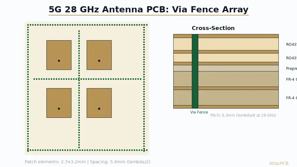
5G FR2 band (28 GHz) phased array antenna PCBs require Rogers RO4350B or RO3003 substrates with tightly controlled dielectric thickness (+/-0.5mil) to maintain element resonant frequency within 200 MHz of target. Via array ground fencing at 0.3mm pitch (lambda/4 at 28 GHz) suppresses surface waves and improves array isolation by 8-12 dB. The critical fabrication challenge is maintaining copper registration accuracy of +/-25um across the array aperture to preserve beam steering accuracy within +/-0.5 degrees.
The Manufacturing Challenge: Antenna Performance Is Fabrication Accuracy
Building a 5G mmWave phased array antenna is fundamentally a precision manufacturing problem, not just a design problem. At 28 GHz, free-space wavelength is 10.7mm — and inside a Rogers 4350B substrate, it shrinks to approximately 5.7mm. That means a quarter-wavelength patch antenna element is only 2.7mm long, and a 1% dimensional error (27um) causes a measurable shift in resonant frequency. This is why material selection, layer registration, and process control dominate the success or failure of 5G antenna PCB fabrication.
In our production experience with 5G FR2 antenna modules, the boards that achieve specification on the first build are those where the designer and manufacturer collaborate on material sourcing and process tolerances before layout. Designs that arrive as completed Gerber files with generic fabrication notes often require 2-3 iterations to achieve acceptable antenna performance — not because the RF design is wrong, but because the fabrication notes did not specify the manufacturing parameters that matter at mmWave frequencies.
Material Selection: Why Rogers 4350B Dominates 5G Antenna PCBs
The FR2 Band Material Requirements
The 5G FR2 frequency bands (24.25-29.5 GHz globally, 26.5-29.5 GHz in many deployments) impose specific material requirements that eliminate most laminate options:
Dk stability across the aperture: A 64-element phased array typically spans 50-80mm. If Dk varies by 2% across this distance, elements at the edges resonate at different frequencies than those at the center — creating gain ripple and beam squint. Rogers 4350B specifies Dk = 3.48 +/-0.05 (1.4% variation), and our incoming inspection data shows actual panel-to-panel variation of +/-0.03 (0.9%). Standard FR-4 with +/-10% Dk variation would create 3-4x the resonant frequency spread across the array.
Loss tangent below 0.005 at 28 GHz: For corporate-fed arrays with 4-8 levels of power splitting, total feed network loss directly reduces array gain. With Rogers 4350B (Df = 0.005 at 28 GHz), a typical 8-element sub-array feed network spanning 35mm experiences approximately 0.8 dB feed loss. Standard FR-4 at Df = 0.020 would give 3.2 dB loss — unacceptable when the antenna gain budget at mmWave is already tight.
Dimensional stability during reflow: 5G active antenna modules undergo lead-free reflow (peak 260C) to attach beamforming ICs and PA/LNA components. The substrate must maintain dimensional stability to prevent antenna element distortion. Rogers 4350B with Tg > 280C and CTE-X/Y of 14/16 ppm/C provides less than 0.01% dimensional change during reflow — versus 0.02-0.04% for standard FR-4 that can shift patch dimensions outside specification.
5G ANTENNA PCB FABRICATION
Rogers 4350B In-Stock for 5G Antenna Builds
We maintain local inventory of RO4350B in 5mil, 6.6mil, 10mil, and 20mil cores. Combined with +/-25um registration accuracy for phased array manufacturing.
Get RF PCB Quote ›
Stackup Design for 5G FR2 Antenna Modules
The Standard Hybrid Antenna Stackup
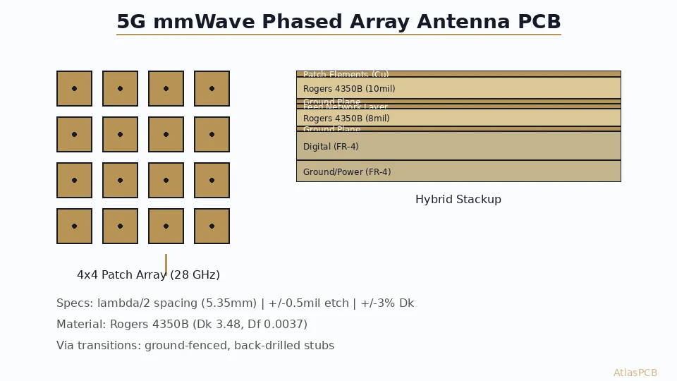
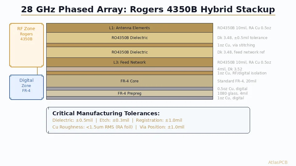
The most common architecture for 5G FR2 active antenna units combines a Rogers antenna layer with FR-4 digital layers in a single 8-12 layer construction:
Layer 1 (Top): Rogers RO4350B, 10mil — Patch antenna elements and microstrip feed network. This layer contains all radiating structures and must maintain the tightest dimensional control.
Layer 2 (Ground): Continuous copper ground plane with via stitching — Serves as both RF ground reference and reflector for the patch antennas. Ground plane quality directly affects antenna efficiency; any discontinuity (slots, thermal reliefs) within the antenna aperture area degrades radiation pattern symmetry.
Layer 3 (Feed/coupling): Rogers RO4350B, 6.6mil — Aperture-coupled feed network or stripline distribution. Used when the antenna architecture separates the radiating element from the excitation feed through a coupling slot in the ground plane.
Layers 4-5 (Power): FR-4, standard thickness — Power distribution for beamforming ICs (typically 1.2V/1.8V core and 3.3V PA supply). Located away from RF layers to avoid coupling.
Layers 6-9 (Digital): FR-4 or Megtron 4 — Digital beamforming control, SPI/I2C buses, and high-speed data interfaces between the antenna module and baseband processor.
Layer 10 (Bottom): FR-4 — BGA mounting surface for beamforming ICs and discrete components.
The Rogers-to-FR-4 transition between layers 3 and 4 is the critical manufacturing junction. We use Rogers RO4450F fusion bonding film (Dk = 3.54 at 10 GHz, matching RO4350B) to bond the Rogers stack to the FR-4 inner core. This prepreg was specifically formulated for Rogers-to-FR-4 transitions and provides 8+ lb/in peel strength after lamination — adequate for the thermal cycling experienced in outdoor antenna installations (-40C to +85C).
Dielectric Thickness Control: The 0.5mil Requirement
For a patch antenna resonant at 28 GHz on 10mil Rogers 4350B, the resonant frequency shifts approximately 10 MHz per 0.1mil of substrate thickness variation. Our specification requires delivered boards to have the antenna substrate layer within +/-0.5mil of nominal — this keeps all elements within a +/-50 MHz window, well inside the typical 5G FR2 channel bandwidth of 100-400 MHz.
Achieving this tolerance requires three process controls that standard multilayer fabrication does not normally maintain:
Incoming material verification: We measure substrate thickness at 9 points per panel on incoming Rogers core material using a precision micrometer. Panels outside +/-0.3mil of nominal are rejected before entering production. Our rejection rate on Rogers material averages 3-5% — higher than FR-4 (which is typically +/-0.5mil as-received).
Lamination pressure uniformity: The hydraulic press must apply uniform pressure across the entire panel to achieve consistent final thickness. Our 4000-ton press with pressure mapping achieves +/-2% pressure uniformity across a 24x18” panel, translating to less than 0.2mil thickness variation from center to edge.
Post-lamination measurement: After pressing, we measure the actual dielectric thickness on test coupons placed at panel corners and center. If measured thickness deviates from nominal by more than 0.5mil, the entire panel is reworked or scrapped. This data also feeds forward into etch compensation — slightly thicker dielectric requires slightly wider traces to maintain target impedance.
Via Array Ground Fencing: Surface Wave Suppression
Why Via Fences Are Critical for Array Performance
In a phased array, surface waves propagating through the substrate between adjacent elements create mutual coupling that degrades scan performance. At 28 GHz, the dominant TM0 surface wave mode in 10mil Rogers 4350B propagates with an effective velocity approximately 70% of free-space speed. Without suppression, this coupling can be -15 to -20 dB between adjacent elements — adequate for some applications but problematic for arrays requiring -25 dB or better element isolation for clean null steering.
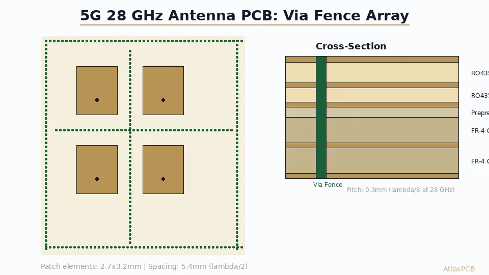
Via fences — dense rows of plated-through vias connecting the top ground plane to the bottom ground plane — create a conductive barrier that blocks surface wave propagation. The effectiveness depends on via pitch relative to the guided wavelength in the substrate.
Design Rules for 28 GHz Via Fences
The maximum via spacing for effective surface wave suppression follows from the resonance condition of the cavity formed between adjacent vias. When via spacing exceeds lambda_g/4 (where lambda_g is the guided wavelength of the surface wave), the fence becomes transparent to propagation. At 28 GHz in Rogers 4350B:
- Guided wavelength (TM0 mode): approximately 6.4mm
- Maximum via pitch for suppression: 1.6mm (lambda_g/4)
- Recommended via pitch: 0.8-1.0mm (lambda_g/8 for robust suppression with manufacturing margin)
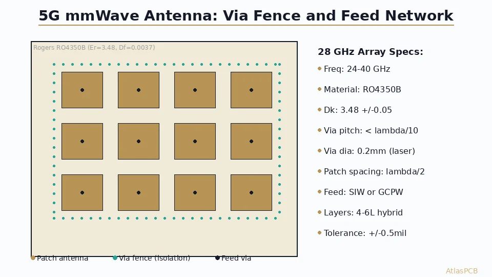
- Optimal via pitch for our process: 0.3mm (using 0.2mm laser-drilled vias)
Using laser-drilled vias at 0.3mm pitch provides approximately 20 dB of additional element isolation compared to un-fenced designs. We have measured this directly on customer arrays using S-parameter extraction between adjacent elements — boards with properly implemented via fencing consistently achieve -30 to -35 dB coupling versus -18 to -22 dB without fencing.
Fabrication Considerations for Dense Via Arrays
Dense via fencing at 0.3mm pitch with 0.2mm via diameter creates specific fabrication challenges:
Drill density and delamination risk: When via density exceeds 30% of the ground plane area, the effective copper removal can create stress concentrations during thermal cycling. Our maximum recommended via density for 10mil substrates is 25% fill factor — corresponding to 0.2mm vias on 0.35mm pitch. At our typical 0.2mm vias on 0.3mm pitch, fill factor is 35%, which is manageable with our specific press profiles but requires reduced lamination pressure (280 PSI vs standard 350 PSI for Rogers) to prevent resin starvation in the via-dense regions.
Via fill requirements: For antenna applications, via fencing vias are typically non-functional electrically (they connect ground to ground) but must be filled to prevent solder wicking during assembly reflow. We use conductive copper fill for these vias, maintaining ground continuity while providing a flat surface for solder mask application.
RF PCB CAPABILITIES
Precision RF Manufacturing for Phased Arrays
+/-25um registration, 0.075mm laser vias, and in-house TDR verification. We fabricate 5G antenna modules for leading infrastructure OEMs.
Registration Accuracy: The Phased Array Precision Problem
How Fabrication Tolerance Affects Beam Steering
In a phased array, the beam is steered by applying progressive phase shifts across the element array. The physical position of each element must match the design position within tight tolerances — otherwise, the actual beam direction deviates from the commanded direction, and sidelobe levels increase.
For a 28 GHz array with 5.4mm element spacing (half-wavelength in free space), the relationship between position error and beam pointing error is approximately:
Beam pointing error (degrees) = arcsin(position_error / (element_spacing x cos(scan_angle)))
At broadside (0 degree scan), a 100um position error creates approximately 1.06 degree beam pointing error. For a single element this is negligible — the array factor averages out random position errors across multiple elements. But systematic errors (like a linear registration drift across the panel) create coherent beam squint that cannot be averaged out.
Our LDI imaging system achieves +/-15um feature-to-feature accuracy within a single exposure field (typically 300x400mm) and +/-25um accuracy across the full 18x24” panel including stitching between exposure fields. For most 5G antenna modules (aperture sizes of 50-100mm), the entire array fits within a single exposure field, meaning element-to-element registration is controlled to +/-15um — providing beam pointing accuracy of +/-0.16 degrees, well within 5G NR specification requirements.
Copper Etching Precision for Antenna Elements
Beyond position accuracy, the antenna element dimensions must be controlled to maintain resonant frequency. A 28 GHz rectangular patch on 10mil RO4350B is approximately 2.7mm x 3.2mm. Standard etch tolerances of +/-1mil (25um) change the element dimensions by less than 1%, shifting resonance by approximately 80 MHz — acceptable for broadband array elements with 3-5% bandwidth.
However, for narrowband elements (filters, diplexers, or series-fed traveling wave arrays), etch tolerance requirements tighten to +/-0.5mil (12.5um). This requires modified etch parameters: reduced conveyor speed, fresh etchant chemistry, and 100% AOI verification of critical dimensions. We provide this “precision etch” service for RF boards at approximately 15-20% cost premium over standard processing.
Quality Verification for 5G Antenna PCBs
What We Measure Before Shipping
For every 5G antenna PCB lot, our RF quality team performs:
Impedance verification (TDR): All feed network traces verified for 50-ohm impedance +/-5%. Test coupons include both microstrip and stripline structures matching the actual board geometry.
Dielectric thickness mapping: Cross-section measurement at 3 locations per panel confirming substrate thickness within +/-0.5mil of nominal.
Registration measurement: Overlay accuracy between copper layers verified using fiducial marks at panel corners. Specification: +/-25um maximum deviation.
Surface roughness: For 28 GHz performance, copper roughness significantly impacts loss. We verify Ra < 0.3um on the RF copper layers using profilometry — this is achieved by using VLP (Very Low Profile) copper foil on the Rogers layers rather than standard electrodeposited copper.
Panel flatness: Warpage measured on a granite surface table. Maximum 0.5% of longest dimension (for a 200mm board, maximum 1.0mm bow) to ensure reliable surface-mount assembly of beamforming ICs.
ATLASPCB
Building a 5G Antenna Module?
We specialize in Rogers-based hybrid constructions for mmWave phased arrays. From prototype to production volume with full RF verification at every stage.
Start Your RF Project ›
Reviewed by AtlasPCB Engineering Team — 15+ years in advanced PCB fabrication for RF, HDI, and rigid-flex applications.
Related Reading:
About AtlasPCB — We specialize in complex PCB manufacturing for HDI, RF, and high-reliability applications. Explore our RF and high-frequency PCB services, Rogers RO4350B PCB manufacturing, or get an multilayer PCB fabrication up to 30 layers . Every order includes free engineering review. Get your quote.
Reviewed by AtlasPCB Engineering Team — IPC-certified manufacturing specialists with 15+ years of production experience in HDI, RF, and high-reliability PCB fabrication. Content based on factory floor data and real customer design reviews.
Frequently Asked Questions
Why is Rogers 4350B preferred over PTFE for 5G antenna PCBs?
What dielectric thickness accuracy is needed for 28 GHz patch antennas?
How close should via fences be for 28 GHz surface wave suppression?
Can a 5G antenna PCB combine Rogers RF layers with FR-4 digital layers?
What registration accuracy is needed for phased array antenna elements?
- 5G antenna PCB fabrication
- Rogers 4350B stackup
- Rogers PCB manufacturer
- China RF PCB manufacturer
- RF PCB design and manufacturing